- 您現(xiàn)在的位置:買賣IC網(wǎng) > PDF目錄67763 > M37920F8CHP 16-BIT, FLASH, 20 MHz, MICROCONTROLLER, PQFP100 PDF資料下載
參數(shù)資料
| 型號: | M37920F8CHP |
| 元件分類: | 微控制器/微處理器 |
| 英文描述: | 16-BIT, FLASH, 20 MHz, MICROCONTROLLER, PQFP100 |
| 封裝: | 14 X 14 MM, 0.50 MM PITCH, PLASTIC, LQFP-100 |
| 文件頁數(shù): | 32/155頁 |
| 文件大小: | 1274K |
| 代理商: | M37920F8CHP |
第1頁第2頁第3頁第4頁第5頁第6頁第7頁第8頁第9頁第10頁第11頁第12頁第13頁第14頁第15頁第16頁第17頁第18頁第19頁第20頁第21頁第22頁第23頁第24頁第25頁第26頁第27頁第28頁第29頁第30頁第31頁當前第32頁第33頁第34頁第35頁第36頁第37頁第38頁第39頁第40頁第41頁第42頁第43頁第44頁第45頁第46頁第47頁第48頁第49頁第50頁第51頁第52頁第53頁第54頁第55頁第56頁第57頁第58頁第59頁第60頁第61頁第62頁第63頁第64頁第65頁第66頁第67頁第68頁第69頁第70頁第71頁第72頁第73頁第74頁第75頁第76頁第77頁第78頁第79頁第80頁第81頁第82頁第83頁第84頁第85頁第86頁第87頁第88頁第89頁第90頁第91頁第92頁第93頁第94頁第95頁第96頁第97頁第98頁第99頁第100頁第101頁第102頁第103頁第104頁第105頁第106頁第107頁第108頁第109頁第110頁第111頁第112頁第113頁第114頁第115頁第116頁第117頁第118頁第119頁第120頁第121頁第122頁第123頁第124頁第125頁第126頁第127頁第128頁第129頁第130頁第131頁第132頁第133頁第134頁第135頁第136頁第137頁第138頁第139頁第140頁第141頁第142頁第143頁第144頁第145頁第146頁第147頁第148頁第149頁第150頁第151頁第152頁第153頁第154頁第155頁
127
M37920F8CGP, M37920F8CHP, M37920FCCGP
M37920FCCHP, M37920FGCGP, M37920FGCHP
PRELIMINAR
Y
Notice:
This
is not
a final
specification.
Some
parametric
limits
are
subject
to change.
SINGLE-CHIP 16-BIT CMOS MICROCOMPUTER FLASH MEMORY VERSION
MITSUBISHI MICROCOMPUTERS
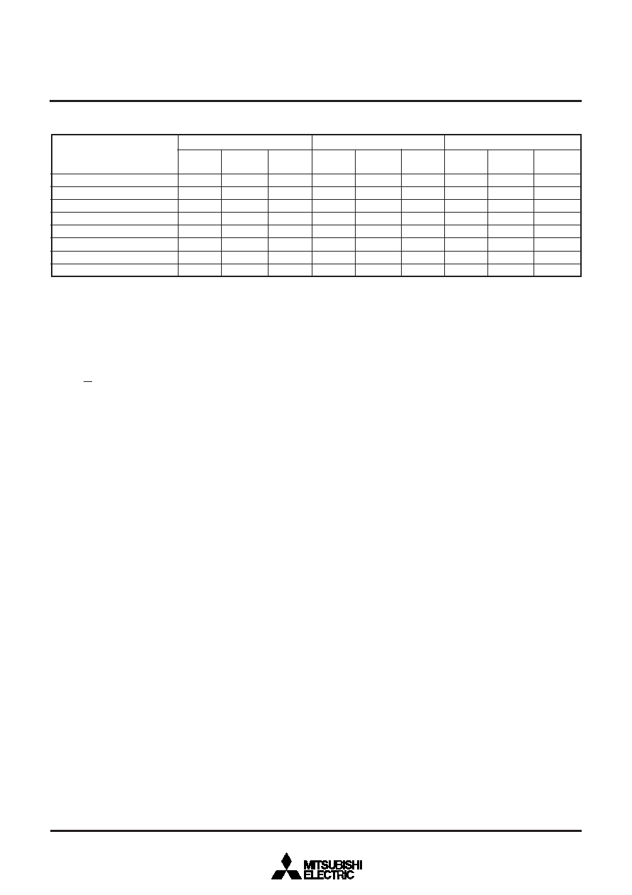
Table 26. Software commands (CPU reprogramming mode)
Command
Read Array
Read Status Register
Clear Status Register
Page Programming (Note 3)
Block Erase
Erase All Unclocked Block
Lock Bit Programming
Read Lock Bit Status
Address
X (Note 2)
X
FF16
7016
5016
4116
2016
A716
7716
7116
1st cycle
2nd cycle
Notes 1: At software commands’ input, the high-order byte of data (D8–D15) is ignored.
2: X = An arbitrary address in the user ROM area. (Note that A0 = “0”.)
3: SRD = Status register data.
4: WA = Write address, WD = Write data (16 bits).
WA and WD must be set from “0016” to “FE16”. (Byte addresses. Incremented by +2. Address A0 = “0”.) Page size = 128 words (128 ! 16 bits).
5: Block address: the maximum address of each block must be input. Note that address A0 = “0”.
6: D6 indicates the block lock status.
“1” = unlocked. “0” = locked.
Mode
Write
3rd cycle
(D0 to D7)
Data
Address
—
X
—
WA0 (Note 4)
BA (Note 5)
X
BA
—
SRD (Note 3)
—
WD0 (Note 4)
D016
D6 (Note 6)
Mode
—
Read
—
Write
Read
Data
Address
—
WA1
—
Mode
—
Write
—
The RY/BY status bit of the flash memory control register goes “0”
during the automatic programming operation; and also, it goes “1” af-
ter the end of it, the same way as bit 7 of the status register.
Reading out the status register after the automatic programming op-
eration is completed reports the result of it. For details, refer to the
section on the status register.
Figure 122 shows an example of the page programming flowchart.
Note that each block can be protected from programming by using a
lock bit. For details, refer to the section on the data protect function.
Additional programming to any page that has already been pro-
grammed is prohibited.
Block Erase Command (2016/D016)
Writing command code "2016" at the 1st bus cycle and writing verify
command code "D016" and the maximum address of the block (Note
that address A0 = “0”.) at the subsequent 2nd bus cycle initiate the
automatic erase (erasing and erase verification) operation for the
specified block.
The completion of the automatic erase operation is verified by a read
of the status register or a read of the flash memory control register.
As the automatic erase operation starts, the microcomputer enters
the read status register mode automatically to allow reading out the
contents of the status register. Bit 7 of the status register (SR.7) is
cleared to “0” simultaneously with the start of the automatic erase
operation; and also, it returns to “1” by the end of it. The read status
register mode is maintained until writing of the read array command
(FF16), writing of the read lock bit status command (7116), or per-
forming the reset operation with the flash memory reset bit.
___
The RY/BY status bit of the flash memory control register goes “0”
during the automatic erase operation; and also, it goes “1” after the
end of it, the same way as bit 7 of the status register.
Reading out the status register after the automatic erase operation
is completed reports the result of it. For details, refer to the section
on the status register.
Figure 123 shows an example of the block erase flowchart.
Note that each block can be protected from erasing by using a lock
Data
—
WD1
—
bit. For details, refer to the section on the data protect function.
相關PDF資料 |
PDF描述 |
|---|---|
| M37920F8CGP | 16-BIT, FLASH, 20 MHz, MICROCONTROLLER, PQFP100 |
| M38039MFL-XXXHP | 8-BIT, MROM, 16.8 MHz, MICROCONTROLLER, PQFP64 |
| M38039MFL-XXXSP | 8-BIT, MROM, 16.8 MHz, MICROCONTROLLER, PDIP64 |
| M38039MFL-XXXWG | 8-BIT, MROM, 16.8 MHz, MICROCONTROLLER, PBGA64 |
| M38039FFLHP | 8-BIT, FLASH, 16.8 MHz, MICROCONTROLLER, PQFP64 |
相關代理商/技術參數(shù) |
參數(shù)描述 |
|---|---|
| M37920FCCGP | 制造商:MITSUBISHI 制造商全稱:Mitsubishi Electric Semiconductor 功能描述:SINGLE-CHIP 16-BIT CMOS MICROCOMPUTER FLASH MEMORY VERSION |
| M37920FCCHP | 制造商:MITSUBISHI 制造商全稱:Mitsubishi Electric Semiconductor 功能描述:SINGLE-CHIP 16-BIT CMOS MICROCOMPUTER FLASH MEMORY VERSION |
| M37920FGCGP | 制造商:MITSUBISHI 制造商全稱:Mitsubishi Electric Semiconductor 功能描述:SINGLE-CHIP 16-BIT CMOS MICROCOMPUTER FLASH MEMORY VERSION |
| M37920FGCHP | 制造商:MITSUBISHI 制造商全稱:Mitsubishi Electric Semiconductor 功能描述:SINGLE-CHIP 16-BIT CMOS MICROCOMPUTER FLASH MEMORY VERSION |
| M37920S4CGP | 制造商:MITSUBISHI 制造商全稱:Mitsubishi Electric Semiconductor 功能描述:16 BIT CMOS MICROCOMPUTER |
發(fā)布緊急采購,3分鐘左右您將得到回復。