- 您現(xiàn)在的位置:買賣IC網(wǎng) > PDF目錄45037 > M37735MHBXXXFP 16-BIT, MROM, 25 MHz, MICROCONTROLLER, PQFP80 PDF資料下載
參數(shù)資料
| 型號(hào): | M37735MHBXXXFP |
| 元件分類: | 微控制器/微處理器 |
| 英文描述: | 16-BIT, MROM, 25 MHz, MICROCONTROLLER, PQFP80 |
| 封裝: | 14 X 20 MM, 0.80 MM PITCH, PLASTIC, QFP-80 |
| 文件頁數(shù): | 52/93頁 |
| 文件大?。?/td> | 1802K |
| 代理商: | M37735MHBXXXFP |
第1頁第2頁第3頁第4頁第5頁第6頁第7頁第8頁第9頁第10頁第11頁第12頁第13頁第14頁第15頁第16頁第17頁第18頁第19頁第20頁第21頁第22頁第23頁第24頁第25頁第26頁第27頁第28頁第29頁第30頁第31頁第32頁第33頁第34頁第35頁第36頁第37頁第38頁第39頁第40頁第41頁第42頁第43頁第44頁第45頁第46頁第47頁第48頁第49頁第50頁第51頁當(dāng)前第52頁第53頁第54頁第55頁第56頁第57頁第58頁第59頁第60頁第61頁第62頁第63頁第64頁第65頁第66頁第67頁第68頁第69頁第70頁第71頁第72頁第73頁第74頁第75頁第76頁第77頁第78頁第79頁第80頁第81頁第82頁第83頁第84頁第85頁第86頁第87頁第88頁第89頁第90頁第91頁第92頁第93頁

53
MITSUBISHI MICROCOMPUTERS
M37735MHBXXXFP
SINGLE-CHIP 16-BIT CMOS MICROCOMPUTER
PRELIMINARY
Notice:
This
is not
a final
specification.
Some
parametric
limits
are
subject
to change.
Single-chip mode
_
E
_
Enable signal E is output.
“L” is output.
___
RDE
,
___
RDE
, WEL, WEH are output when the
___
RDE
, WEL, WEH are output only when the
___
WEL
, WEH
internal/external memory area is accessed.
external memory area is accessed.
“L” is output after WIT/STP instruction is
executed.
Standby state selection bit (bit 0 of port
function control register) must be set
to “1”.
“H”or “L” is output. (Output the content of
P42 latch.)
Port P42 direction register must be set to
“1”.
00 100016
to
00 7FFF16
02 000016 (Note)
00 800016
to
03 FFFF16
04 000016
to
07 FFFF16
08 000016
to
0B FFFF16
0C 000016
to
0F FFFF16
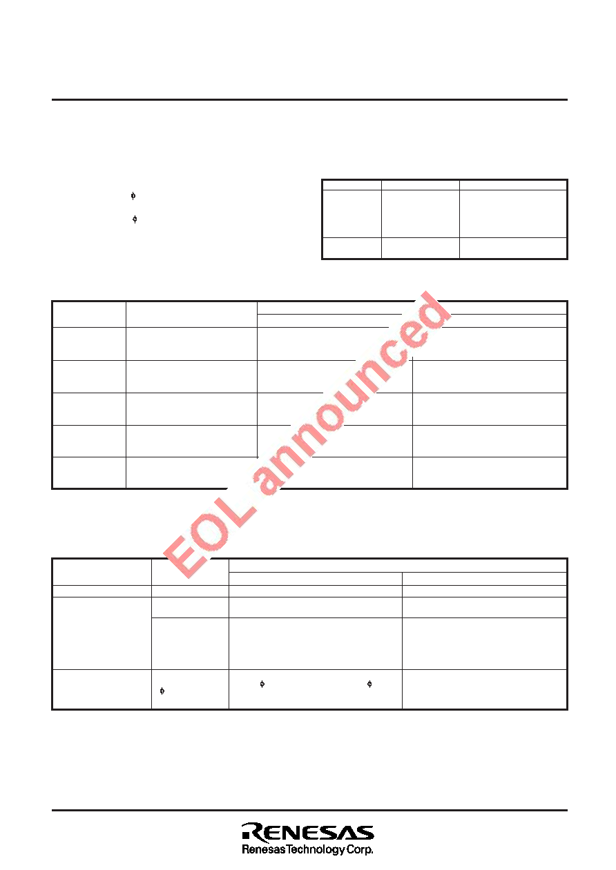
Table 9 shows the relationship between the CNVss pin input level
and the processor modes.
Table 9. Relationship between CNVss pin input levels and processor
modes
CNVss
Mode
Description
Single-chip mode upon
starting after reset. Each
mode can be selected by
changing the processor
mode bits by software.
Microprocessor mode upon
starting after reset.
Single-chip
Memory expansion
Microprocessor
Vss
Vcc
___
Table 7. Relationship between access addresses and chip-select signals CS0 to CS4
Access address
Memory expansion mode
Microprocessor mode
Chip-select
signal
Area
Note. This applies when both bits 1 and 0 of the memory allocation control register is “0”. Refer to on the section ROM AREA MODIFICATION
FUNCTION.
Table 8. Function of signal output disable selection bit CM6 (bit 6 of oscillation circuit control register 0)
Function
CM6 = “0”
CM6 = “1”
Processor mode
Pin
The latter half of bank 0016 except
for internal memory area and
banks 0116 to 0316.
Banks 0416 to 0716
Banks 0816 to 0B16
Banks 0C16 to 0F16
The first half of bank 0016 except
for internal momory area
___
CS0
___
CS1
___
CS2
___
CS3
___
CS4
(3) Microprocessor mode [10]
Microprocessor mode is entered by connecting the CNVss pin to Vcc
and starting from reset. It can also be entered by programming the
processor mode bits to “10” after connecting the CNVss pin to Vss
and starting from reset. This mode is similar to the memory expansion
mode except that internal ROM is disabled and an external memory
is required, and clock
1
from port P42 is always output independently
of bit 7 of the processor mode register 0.
As shown in Table 8,
1
output can also be stopped with the signal
output disable selection bit “1”. In this case, write “1” to the port P42
direction register.
___
RDE
Memory expansion mode,
Microprocessor mode
1
Note. Functions shown in Table 7 cannot be emulated in a debugger. For the oscillation circuit control register 0, refer to Figure 63.
For the port function control register, refer to Figure 11.
—————
Clock
1
is output independent of
1
output selection bit.
After WIT/STP instruction is executed,
“H” is output.
相關(guān)PDF資料 |
PDF描述 |
|---|---|
| M37735MHLXXXHP | 16-BIT, MROM, 12 MHz, MICROCONTROLLER, PQFP80 |
| M37735S4LHP | 16-BIT, 12 MHz, MICROCONTROLLER, PQFP80 |
| M37736EHBGS | 16-BIT, UVPROM, 24 MHz, MICROCONTROLLER, CQCC100 |
| M37736EHBXXXGP | 16-BIT, OTPROM, 25 MHz, MICROCONTROLLER, PQFP100 |
| M37736EHBGS | 16-BIT, UVPROM, 25 MHz, MICROCONTROLLER, CQCC100 |
相關(guān)代理商/技術(shù)參數(shù) |
參數(shù)描述 |
|---|---|
| M37735MHL | 制造商:MITSUBISHI 制造商全稱:Mitsubishi Electric Semiconductor 功能描述:SINGLE-CHIP 16-BIT CMOS MICROCOMPUTER |
| M37735MHL-143HP | 制造商:MITSUBISHI 制造商全稱:Mitsubishi Electric Semiconductor 功能描述:PROM VERSION OF M37735MHLXXXHP |
| M37735MHLXXXHP | 制造商:RENESAS 制造商全稱:Renesas Technology Corp 功能描述:SINGLE-CHIP 16-BIT CMOS MICROCOMPUTER |
| M37735S4BFP | 制造商:RENESAS 制造商全稱:Renesas Technology Corp 功能描述:16-BIT CMOS MICROCOMPUTER |
| M37735S4LHP | 制造商:RENESAS 制造商全稱:Renesas Technology Corp 功能描述:16-BIT CMOS MICROCOMPUTER |
發(fā)布緊急采購,3分鐘左右您將得到回復(fù)。