- 您現(xiàn)在的位置:買賣IC網(wǎng) > PDF目錄69009 > M30240M5-XXXFP 16-BIT, MROM, 12 MHz, MICROCONTROLLER, PQFP80 PDF資料下載
參數(shù)資料
| 型號(hào): | M30240M5-XXXFP |
| 元件分類: | 微控制器/微處理器 |
| 英文描述: | 16-BIT, MROM, 12 MHz, MICROCONTROLLER, PQFP80 |
| 封裝: | 0.80 MM PITCH, PLASTIC, QFP-80 |
| 文件頁(yè)數(shù): | 132/139頁(yè) |
| 文件大小: | 1453K |
| 代理商: | M30240M5-XXXFP |
第1頁(yè)第2頁(yè)第3頁(yè)第4頁(yè)第5頁(yè)第6頁(yè)第7頁(yè)第8頁(yè)第9頁(yè)第10頁(yè)第11頁(yè)第12頁(yè)第13頁(yè)第14頁(yè)第15頁(yè)第16頁(yè)第17頁(yè)第18頁(yè)第19頁(yè)第20頁(yè)第21頁(yè)第22頁(yè)第23頁(yè)第24頁(yè)第25頁(yè)第26頁(yè)第27頁(yè)第28頁(yè)第29頁(yè)第30頁(yè)第31頁(yè)第32頁(yè)第33頁(yè)第34頁(yè)第35頁(yè)第36頁(yè)第37頁(yè)第38頁(yè)第39頁(yè)第40頁(yè)第41頁(yè)第42頁(yè)第43頁(yè)第44頁(yè)第45頁(yè)第46頁(yè)第47頁(yè)第48頁(yè)第49頁(yè)第50頁(yè)第51頁(yè)第52頁(yè)第53頁(yè)第54頁(yè)第55頁(yè)第56頁(yè)第57頁(yè)第58頁(yè)第59頁(yè)第60頁(yè)第61頁(yè)第62頁(yè)第63頁(yè)第64頁(yè)第65頁(yè)第66頁(yè)第67頁(yè)第68頁(yè)第69頁(yè)第70頁(yè)第71頁(yè)第72頁(yè)第73頁(yè)第74頁(yè)第75頁(yè)第76頁(yè)第77頁(yè)第78頁(yè)第79頁(yè)第80頁(yè)第81頁(yè)第82頁(yè)第83頁(yè)第84頁(yè)第85頁(yè)第86頁(yè)第87頁(yè)第88頁(yè)第89頁(yè)第90頁(yè)第91頁(yè)第92頁(yè)第93頁(yè)第94頁(yè)第95頁(yè)第96頁(yè)第97頁(yè)第98頁(yè)第99頁(yè)第100頁(yè)第101頁(yè)第102頁(yè)第103頁(yè)第104頁(yè)第105頁(yè)第106頁(yè)第107頁(yè)第108頁(yè)第109頁(yè)第110頁(yè)第111頁(yè)第112頁(yè)第113頁(yè)第114頁(yè)第115頁(yè)第116頁(yè)第117頁(yè)第118頁(yè)第119頁(yè)第120頁(yè)第121頁(yè)第122頁(yè)第123頁(yè)第124頁(yè)第125頁(yè)第126頁(yè)第127頁(yè)第128頁(yè)第129頁(yè)第130頁(yè)第131頁(yè)當(dāng)前第132頁(yè)第133頁(yè)第134頁(yè)第135頁(yè)第136頁(yè)第137頁(yè)第138頁(yè)第139頁(yè)
92
Mitsubishi microcomputers
M30240 Group
SINGLE-CHIP 16-BIT CMOS MICROCOMPUTER
Specifications REV. G
Specifications in this manual are tentative and subject to change
UART0 to UART2
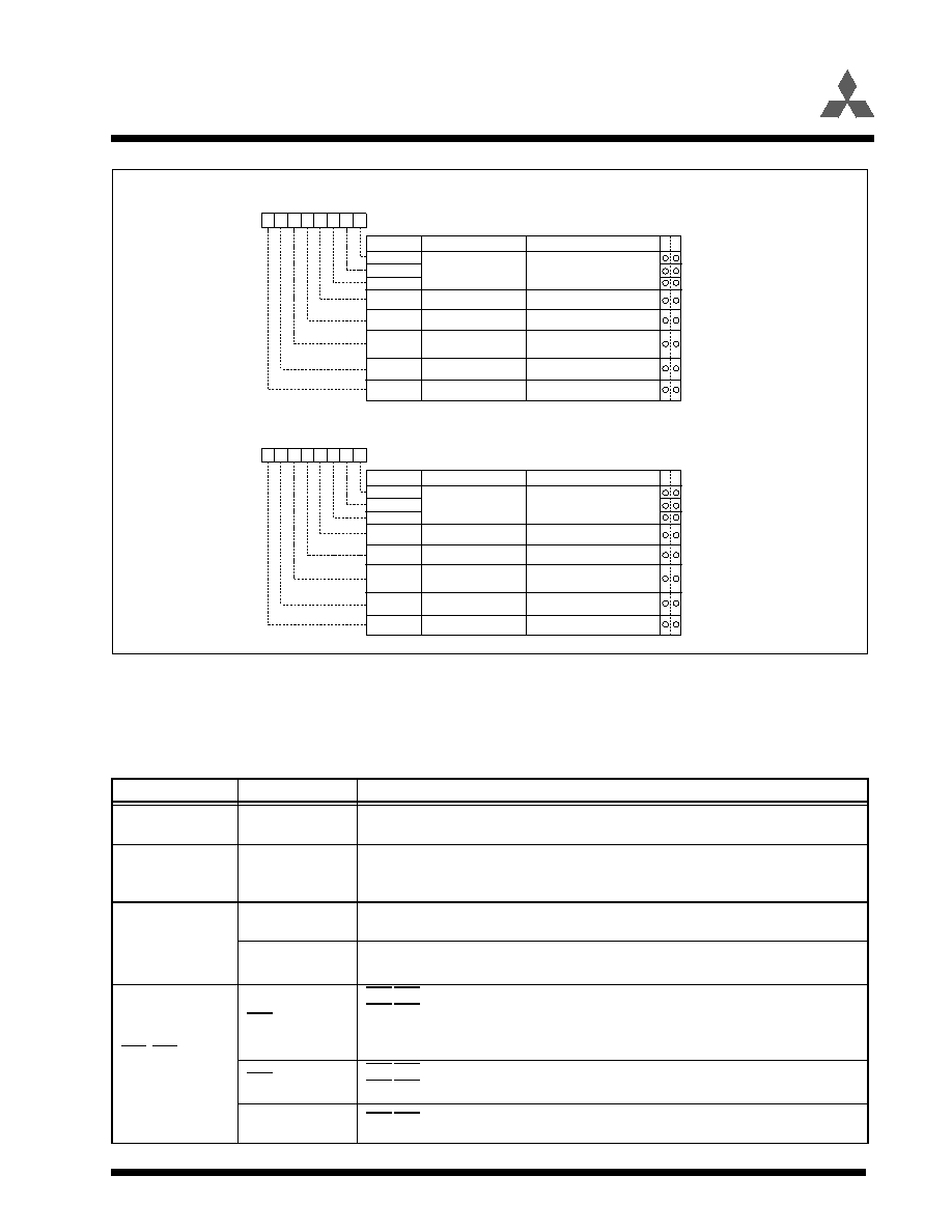
Figure 1.87: UARTi transmit/receive mode register.
Table 1.28 lists the functions of the input/output pins during UART mode. Note that for a period from
when the UARTi operation mode is selected to when transfer starts, the TxDi pin outputs a “H”.
Table 1.28:
Input/output pin functions in UART mode
Pin name
Function
Method of selection
TxDi
(P63, P67, P70)
Serial data
output
Outputs dummy data when performing reception.
RxDi
(P62, P66, P71)
Serial data input
Port P62, P66, and P71 direction register (bits 2 and 6 at address 03EE16 bit 1 at address
03EF16)= “0”
(Can be used as an input port when performing transmission only.)
CLKi
(P61, P65, P72)
Programmable I/
O port
Internal/external clock select bit (bit 3 at address 03A016, 03A816, 037816) = “0”
Transfer clock
input
Internal/external clock select bit (bit 3 at address 03A016, 03A816) = “1”
Port P61, P65 direction register (bits 1 and 5 at address 03EE16) = “0”
CTSi/RTSi
(P60,P64,P73)
CTS input
CTS/RTS disable bit (bit 4 at address 03A416, 03AC16, 037C16) = “0”
CTS/RTS function select bit (bit 2 at address 03A416, 03AC16, 037C16) = “0”
Port P60, P64 and P73 direction register (bits 0 and 4 at address 03EE16, bit 3 at address
03EF16) = “0”
RTS output
CTS/RTS disable bit (bit 4 at address 03A416, 03AC16, 037C16) = “0”
CTS/RTS function select bit (bit 2 at address 03A416, 03AC16, 037C16) = “1”
Programmable I/
O port
CTS/RTS disable bit (bit 4 at address 03A416, 03AC16, 037C16) = “1”
Symbol
Address
When reset
UiMR(i=0,1)
03A016, 03A816
0016
CKDIR
UARTi transmit / receive mode registers
Internal / external clock
select bit
STPS
PRY
PRYE
SLEP
0 : Internal clock
1 : External clock (Note)
Bit name
Function
Bit symbol
W
R
b7
b6
b5
b4
b3
b2
b1
b0
SMD0
SMD1
SMD2
Serial I/O mode select bit
b2 b1 b0
0 : One stop bit
1 : Two stop bits
0 : Parity disabled
1 : Parity enabled
0 : Sleep mode deselected
1 : Sleep mode selected
1 0 0 : Transfer data 7 bits long
1 0 1 : Transfer data 8 bits long
1 1 0 : Transfer data 9 bits long
Valid when bit 6 = “1”
0 : Odd parity
1 : Even parity
Stop bit length select bit
Odd / even parity
select bit
Parity enable bit
Sleep select bit
Symbol
Address
When reset
U2MR
037816
0016
CKDIR
UART2 transmit / receive mode register
Internal / external clock
select bit
STPS
PRY
PRYE
IOPOL
Must always be fixed to “0”
Bit name
Function
Bit symbol
W
R
b7
b6
b5
b4
b3
b2
b1
b0
SMD0
SMD1
SMD2
Serial I/O mode select bit
b2 b1 b0
0 : One stop bit
1 : Two stop bits
0 : Parity disabled
1 : Parity enabled
0 : No reverse
1 : Reverse
1 0 0 : Transfer data 7 bits long
1 0 1 : Transfer data 8 bits long
1 1 0 : Transfer data 9 bits long
Valid when bit 6 = “1”
0 : Odd parity
1 : Even parity
Stop bit length select bit
Odd / even parity
select bit
Parity enable bit
TxD, RxD I/O polarity
reverse bit (Note)
Note: Usually set to “0”.
Note: Set the corresponding port direction register to "0".
相關(guān)PDF資料 |
PDF描述 |
|---|---|
| M30240M6-XXXXFP | 16-BIT, MROM, 12 MHz, MICROCONTROLLER, PQFP80 |
| M30240ECFP | 16-BIT, OTPROM, 12 MHz, MICROCONTROLLER, PQFP80 |
| M30240M5-XXXXFP | 16-BIT, MROM, 12 MHz, MICROCONTROLLER, PQFP80 |
| M30240M6-XXXXFP | 16-BIT, OTPROM, MICROCONTROLLER, PQFP80 |
| M30240ECFP | 16-BIT, OTPROM, MICROCONTROLLER, PQFP80 |
相關(guān)代理商/技術(shù)參數(shù) |
參數(shù)描述 |
|---|---|
| M30240M6 | 制造商:MITSUBISHI 制造商全稱:Mitsubishi Electric Semiconductor 功能描述:SINGLE-CHIP 16-BIT CMOS MICROCOMPUTER |
| M30240M6-XXXFP | 制造商:MITSUBISHI 制造商全稱:Mitsubishi Electric Semiconductor 功能描述:SINGLE-CHIP 16-BIT CMOS MICROCOMPUTER |
| M30240M7 | 制造商:MITSUBISHI 制造商全稱:Mitsubishi Electric Semiconductor 功能描述:SINGLE-CHIP 16-BIT CMOS MICROCOMPUTER |
| M30240M7-XXXFP | 制造商:MITSUBISHI 制造商全稱:Mitsubishi Electric Semiconductor 功能描述:SINGLE-CHIP 16-BIT CMOS MICROCOMPUTER |
| M30240M8 | 制造商:MITSUBISHI 制造商全稱:Mitsubishi Electric Semiconductor 功能描述:SINGLE-CHIP 16-BIT CMOS MICROCOMPUTER |
發(fā)布緊急采購(gòu),3分鐘左右您將得到回復(fù)。