- 您現(xiàn)在的位置:買賣IC網(wǎng) > PDF目錄377800 > M12L2561616A-6BG (ELITE SEMICONDUCTOR MEMORY TECHNOLOGY INC) 4M x 16 Bit x 4 Banks Synchronous DRAM PDF資料下載
參數(shù)資料
| 型號: | M12L2561616A-6BG |
| 廠商: | ELITE SEMICONDUCTOR MEMORY TECHNOLOGY INC |
| 元件分類: | DRAM |
| 英文描述: | 4M x 16 Bit x 4 Banks Synchronous DRAM |
| 中文描述: | 16M X 16 SYNCHRONOUS DRAM, 5.4 ns, PBGA54 |
| 封裝: | 8 X 13 MM, LEAD FREE, BGA-54 |
| 文件頁數(shù): | 6/44頁 |
| 文件大小: | 908K |
| 代理商: | M12L2561616A-6BG |
第1頁第2頁第3頁第4頁第5頁當前第6頁第7頁第8頁第9頁第10頁第11頁第12頁第13頁第14頁第15頁第16頁第17頁第18頁第19頁第20頁第21頁第22頁第23頁第24頁第25頁第26頁第27頁第28頁第29頁第30頁第31頁第32頁第33頁第34頁第35頁第36頁第37頁第38頁第39頁第40頁第41頁第42頁第43頁第44頁
ES MT
M12L2561616A
Elite Semiconductor Memory Technology Inc.
Revision
:
1.2
Publication Date
:
Aug. 2007
6/44
Version
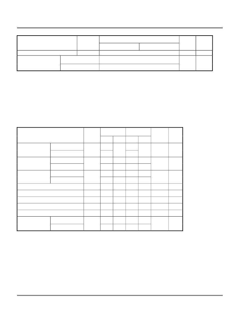
Parameter
Symbol
-6
-7
Unit
Note
Col. address to col. address delay
t
CCD(min)
1
t
CK
3
CAS latency = 3
2
Number of valid
Output data
CAS latency = 2
1
ea
4
Note : 1. The minimum number of clock cycles is determined by dividing the minimum time required with clock cycle time and then
rounding off to the next higher integer.
2. Minimum delay is required to complete write.
3. All parts allow every cycle column address change.
4. In case of row precharge interrupt, auto precharge and read burst stop.
5. A new command may be given t
RFC
after self refresh exit.
6. A maximum of eight consecutive AUTO REFRESH commands (with t
RFCmin
) can be posted to any given SDRAM, and the
maximum absolute interval between any AUTO REFRESH command and the next AUTO REFRESH command is
8x7.8
μ
s.)
AC CHARACTERISTICS
(AC operating condition unless otherwise noted)
-6
-7
Parameter
Symbol
MIN
MAX
MIN
MAX
Unit
Note
CAS latency = 3
6
7
CLK cycle time
CAS latency = 2
t
CC
10
1000
10
1000
ns
1
CAS latency = 3
-
5.4
-
5.4
CLK to valid
output delay
CAS latency = 2
t
SAC
-
5.4
-
5.4
ns
1,2
CAS latency = 3
2.5
-
3
-
Output data
hold time
CAS latency = 2
t
OH
-
-
3
-
ns
2
CLK high pulsh width
t
CH
2.5
-
2.5
-
ns
3
CLK low pulsh width
t
CL
2.5
-
2.5
-
ns
3
Input setup time
t
SS
1.5
-
1.5
-
ns
3
Input hold time
t
SH
1
-
1
-
ns
3
CLK to output in Low-Z
t
SLZ
1
-
1
-
ns
2
CAS latency = 3
-
5.4
-
5.4
CLK to output
in Hi-Z
CAS latency = 2
t
SHZ
-
6
-
6
ns
-
Note : 1. Parameters depend on programmed CAS latency.
2. If clock rising time is longer than 1ns. (tr/2 - 0.5) ns should be considered.
3. Assumed input rise and fall time (tr & tf) =1ns.
If tr & tf is longer than 1ns. transient time compensation should be considered.
i.e., [(tr + tf)/2 – 1] ns should be added to the parameter.
相關PDF資料 |
PDF描述 |
|---|---|
| M12L2561616A-6TG | 4M x 16 Bit x 4 Banks Synchronous DRAM |
| M12L2561616A-7BG | 4M x 16 Bit x 4 Banks Synchronous DRAM |
| M12L2561616A-7TG | 4M x 16 Bit x 4 Banks Synchronous DRAM |
| M12L32162A | 1M x 16Bit x 2Banks Synchronous DRAM |
| M12L32162A-7BG | 1M x 16Bit x 2Banks Synchronous DRAM |
相關代理商/技術參數(shù) |
參數(shù)描述 |
|---|---|
| M12L2561616A-6BG2K | 制造商:ESMT 制造商全稱:Elite Semiconductor Memory Technology Inc. 功能描述:JEDEC standard 3.3V power supply |
| M12L2561616A-6BIG | 制造商:ESMT 制造商全稱:Elite Semiconductor Memory Technology Inc. 功能描述:4M x 16 Bit x 4 Banks Synchronous DRAM |
| M12L2561616A-6TG | 制造商:ESMT 制造商全稱:Elite Semiconductor Memory Technology Inc. 功能描述:4M x 16 Bit x 4 Banks Synchronous DRAM |
| M12L2561616A-6TG2K | 制造商:ESMT 制造商全稱:Elite Semiconductor Memory Technology Inc. 功能描述:JEDEC standard 3.3V power supply |
| M12L2561616A-6TIG | 制造商:ESMT 制造商全稱:Elite Semiconductor Memory Technology Inc. 功能描述:4M x 16 Bit x 4 Banks Synchronous DRAM |
發(fā)布緊急采購,3分鐘左右您將得到回復。