- 您現(xiàn)在的位置:買賣IC網(wǎng) > PDF目錄378652 > LXT974 (Intel Corp.) Fast Ethernet 10/100 Quad Transceivers PDF資料下載
參數(shù)資料
| 型號(hào): | LXT974 |
| 廠商: | Intel Corp. |
| 英文描述: | Fast Ethernet 10/100 Quad Transceivers |
| 中文描述: | 四10/100快速以太網(wǎng)收發(fā)器 |
| 文件頁數(shù): | 50/74頁 |
| 文件大小: | 1089K |
| 代理商: | LXT974 |
第1頁第2頁第3頁第4頁第5頁第6頁第7頁第8頁第9頁第10頁第11頁第12頁第13頁第14頁第15頁第16頁第17頁第18頁第19頁第20頁第21頁第22頁第23頁第24頁第25頁第26頁第27頁第28頁第29頁第30頁第31頁第32頁第33頁第34頁第35頁第36頁第37頁第38頁第39頁第40頁第41頁第42頁第43頁第44頁第45頁第46頁第47頁第48頁第49頁當(dāng)前第50頁第51頁第52頁第53頁第54頁第55頁第56頁第57頁第58頁第59頁第60頁第61頁第62頁第63頁第64頁第65頁第66頁第67頁第68頁第69頁第70頁第71頁第72頁第73頁第74頁
LXT974/LXT975
—
Fast Ethernet 10/100 Quad Transceivers
50
Datasheet
4.0
Test Specifications
Note:
The minimum and maximum values in
Table 22
through
Table 42
and
Figure 26
through
Figure 39
represent the performance specifications of the LXT974/975 and are guaranteed by test, except
where noted by design. Minimum and maximum values in
Table 24
through
Table 42
apply over
the recommended operating conditions specific in
Table 23
.
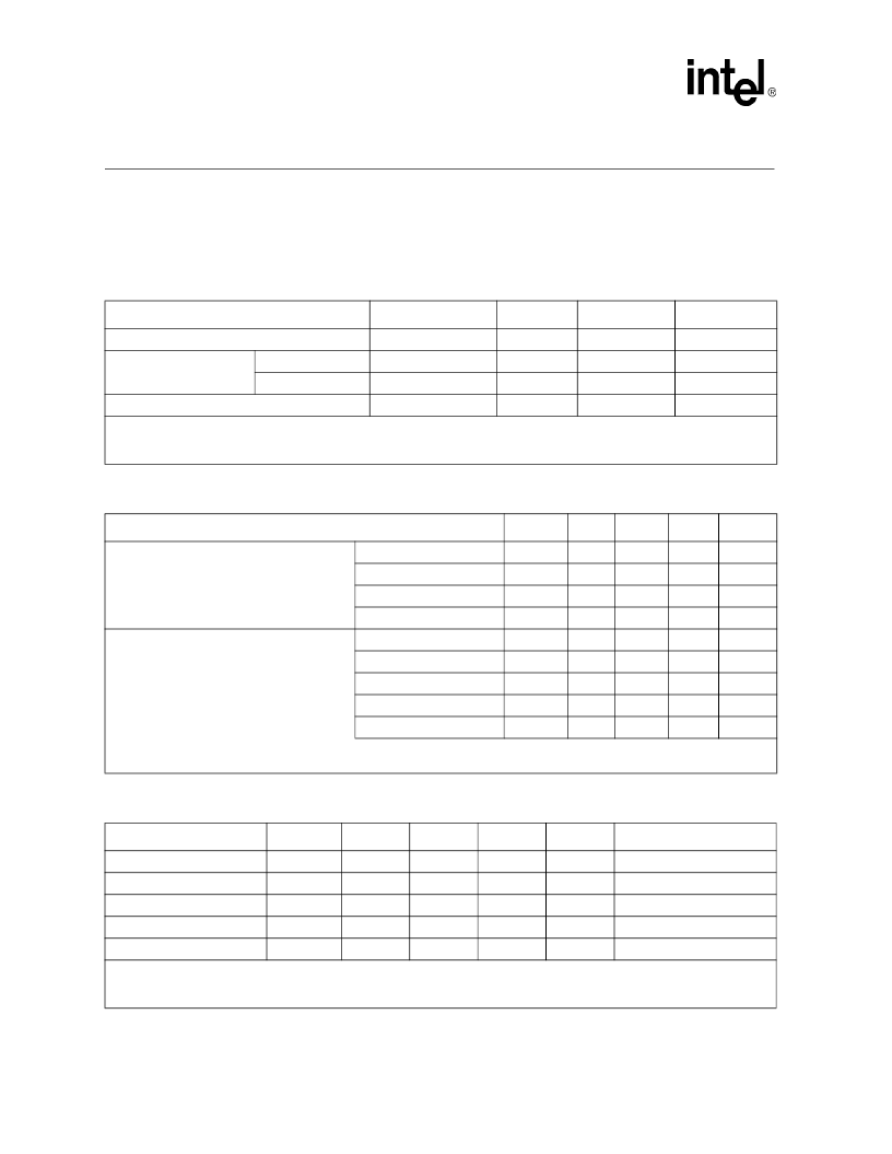
Table 22. Absolute Maximum Ratings
Parameter
Sym
Min
Max
Units
Supply voltage
V
CC
-0.3
6
V
Operating temperature
Ambient
T
OPA
-15
+85
o
C
Case
T
OPC
–
+120
o
C
Storage temperature
T
ST
-65
+150
o
C
Caution:
Exceeding these values may cause permanent damage.
Functional operation under these conditions is not implied.
Exposure to maximum rating conditions for extended periods may affect device reliability.
Table 23. Operating Conditions
Parameter
Sym
Min
Typ
1
Max
Units
Recommended supply voltage
2
Except MII Supply
Vcc
4.75
5.0
5.25
V
MII Supply
V
CC
MII
3.125
–
5.25
V
Recommended operating temperature
Ambient
T
OPA
0
–
70
o
C
Case
T
OPC
0
–
110
o
C
V
CC
current
100BASE-TX
I
CC
–
–
570
mA
100BASE-FX
I
CC
–
–
500
mA
10BASE-T
I
CC
–
–
570
mA
Power Down Mode
I
CC
–
0.5
3.0
mA
Auto-Negotiation
I
CC
–
–
570
mA
1. Typical values are at 25
°
C and are for design aid only; not guaranteed and not subject to production testing.
2. Voltages with respect to ground unless otherwise specified.
Table 24. Digital I/O Characteristics
1
Parameter
Symbol
Min
Typ
2
Max
Units
Test Conditions
Input Low voltage
3
V
IL
–
–
0.8
V
–
Input High voltage
3
V
IH
2.0
–
–
V
–
Input current
I
I
-100
–
100
μ
A
0.0 < V
I
< V
CC
Output Low voltage
V
OL
–
–
0.4
V
I
OL
= 4 mA
Output High voltage
V
OH
2.4
–
–
V
I
OH
= -4 mA
1. Applies to all pins except MII pins. Refer to
Table 25
for MII I/O Characteristics.
2. Typical values are at 25
°
C and are for design aid only; not guaranteed and not subject to production testing.
3. Does not apply to CLK25M. Refer to
Table 26
for clock input levels.
相關(guān)PDF資料 |
PDF描述 |
|---|---|
| LXT974A | Fast Ethernet 10/100 Quad Transceivers |
| LXT974AHC | Fast Ethernet 10/100 Quad Transceivers |
| LXT974B | Fast Ethernet 10/100 Quad Transceivers |
| LXT974BHC | Fast Ethernet 10/100 Quad Transceivers |
| LXT975 | Fast Ethernet 10/100 Quad Transceivers |
相關(guān)代理商/技術(shù)參數(shù) |
參數(shù)描述 |
|---|---|
| LXT974A | 制造商:INTEL 制造商全稱:Intel Corporation 功能描述:Fast Ethernet 10/100 Quad Transceivers |
| LXT974AHC | 制造商:INTEL 制造商全稱:Intel Corporation 功能描述:Fast Ethernet 10/100 Quad Transceivers |
| LXT974B | 制造商:INTEL 制造商全稱:Intel Corporation 功能描述:Fast Ethernet 10/100 Quad Transceivers |
| LXT974BHC | 制造商:INTEL 制造商全稱:Intel Corporation 功能描述:Fast Ethernet 10/100 Quad Transceivers |
| LXT974QC | 制造商:LEVELONE 功能描述: |
發(fā)布緊急采購,3分鐘左右您將得到回復(fù)。