- 您現(xiàn)在的位置:買(mǎi)賣(mài)IC網(wǎng) > PDF目錄358941 > LRS1341 (Sharp Corporation) Stacked Chip 16M Flash Memory and 2M SRAM PDF資料下載
參數(shù)資料
| 型號(hào): | LRS1341 |
| 廠商: | Sharp Corporation |
| 英文描述: | Stacked Chip 16M Flash Memory and 2M SRAM |
| 中文描述: | 堆疊芯片1,600快閃記憶體以及2M SRAM |
| 文件頁(yè)數(shù): | 4/24頁(yè) |
| 文件大?。?/td> | 197K |
| 代理商: | LRS1341 |
第1頁(yè)第2頁(yè)第3頁(yè)當(dāng)前第4頁(yè)第5頁(yè)第6頁(yè)第7頁(yè)第8頁(yè)第9頁(yè)第10頁(yè)第11頁(yè)第12頁(yè)第13頁(yè)第14頁(yè)第15頁(yè)第16頁(yè)第17頁(yè)第18頁(yè)第19頁(yè)第20頁(yè)第21頁(yè)第22頁(yè)第23頁(yè)第24頁(yè)
LRS1341/LRS1342
Stacked Chip (16M Flash & 2M SRAM)
4
Data Sheet
NOTES:
1. L = V
IL
, H = V
IH
, X = H or L. Refer to DC Characteristics.
2. Refer to the
‘
Flash Memory Command Definition
’
section for valid
D
IN
during a write operation.
3. F-WP set to V
IL
or V
IH
.
4. SRAM standby mode. See Table 2a.
5. Command writes involving block erase or word write are reliably
executed when F-V
PP
= V
PPH
and F-V
CC
= 2.7 V to 3.6 V. Block
erase or word write with V
IH
< RP < V
HH
produce spurious results
and should not be attempted.
6. Never hold F-OE LOW and F-WE LOW at the same time.
7. S-LB, S-UB control mode. See Table 2b.
NOTES:
1. Commands other than those shown in table are reserved by
SHARP for future device implementations and should not be used.
2. BUS operations are defined in Table 2.
3. XA = Any valid address within the device;
IA = Identifier code address;
BA = Address within the block being erased;
WA = Address of memory location to be written;
SRD = Data read from status register, see Table 6;
WD = Data to be written at location WA. Data is latched on the
rising edge of F-WE or F-CE (whichever goes high first);
ID = Data read from identifier codes.
4. See Table 4 for Identifier Codes.
5. See Table 5 for Write Protection Alternatives.
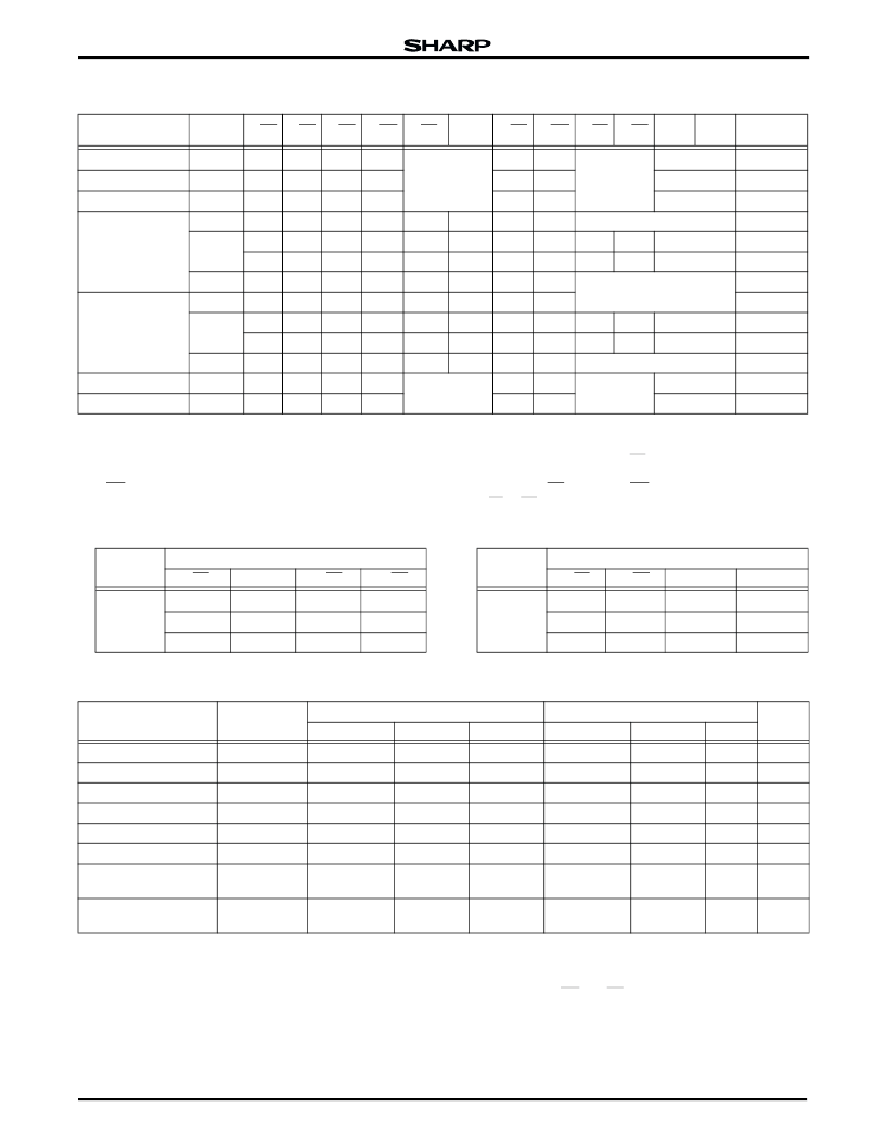
Table 2. Truth Table
1
FLASH
SRAM
F-CE
F-RP
F-OE
F-WE
S-CE
1
S-CE
2
S-OE
S-WE
S-LB
S-UB
DQ
0
-
DQ-7
DQ
8
-
DQ
15
NOTES
Read
Standby
L
H
L
H
See Note 4
X
X
See Note 4
D
OUT
HIGH-Z
2, 3
Output Disable
Standby
L
H
H
H
X
X
3
Write
Standby
L
H
H
L
X
X
D
IN
2, 3, 5, 6
Standby
Read
H
H
X
X
L
H
L
H
See Note 7
Output
Disable
H
H
X
X
L
H
H
H
X
X
HIGH-Z
H
H
X
X
L
H
X
X
H
H
HIGH-Z
Write
H
H
X
X
L
H
L
L
See Note 7
Reset/Power Down
Read
X
L
X
X
L
H
L
H
Output
Disable
X
L
X
X
L
H
H
H
X
X
HIGH-Z
X
L
X
X
L
H
X
X
H
H
HIGH-Z
Write
X
L
X
X
L
H
L
L
See Note 7
Standby
Standby
H
H
X
X
See Note 4
X
X
See Note 4
HIGH-Z
3
Reset/Power Down
Standby
X
L
X
X
X
X
HIGH-Z
3
Table 2a.
MODE
PINS
S-CE
1
S-CE
2
S-LB
S-UB
Standby
(SRAM)
H
X
X
X
X
L
X
X
X
X
H
H
Table 2b.
MODE
(SRAM)
PINS
S-LB
S-UB
DQ
0
- DQ
7
DQ
8
- DQ
15
Read/Write
L
L
D
OUT
/D
IN
D
OUT
/D
IN
HIGH-Z
D
OUT
/D
IN
HIGH-Z
L
H
H
L
D
OUT
/D
IN
Table 3. Command Definition for Flash Memory
1
COMMAND
BUS CYCLES
REQUIRED
FIRST BUS CYCLE
ADDRESS
3
SECOND BUS CYCLE
OPERATION
2
NOTES
OPERATION
2
DATA
3
ADDRESS
3
DATA
3
Read Array/Reset
1
Write
XA
FFH
Read Identifier Codes
≥
2
Write
XA
90H
Read
IA
ID
4
Read Status Register
2
Write
XA
70H
Read
XA
SRD
Clear Status Register
1
Write
XA
50H
Block Erase
2
Write
BA
20H
Write
BA
D0H
5
Word Write
2
Write
WA
40H or 10H
Write
WA
WD
5
Block Erase and Word
Write Suspend
1
Write
XA
B0H
5
Block Erase and Word
Write Resume
1
Write
XA
D0H
5
相關(guān)PDF資料 |
PDF描述 |
|---|---|
| LRS1805A | Stacked Chip 64M (x16) Flash Memory + 16M (x16) Smartcombo RAM |
| LRS250 | LIGHT EMITTING DIODES |
| LRS250-DO | LIGHT EMITTING DIODES |
| LRZ180-CO | Array LED 2 mm LED, Diffused |
| LS-3101S | Thyratrons |
相關(guān)代理商/技術(shù)參數(shù) |
參數(shù)描述 |
|---|---|
| LRS1342 | 制造商:Sharp Microelectronics Corporation 功能描述:COMBO 1MX16 FLASH + 128KX16 SRAM 2.7V TO 3.6V 72FBGA - Trays |
| LRS1348 | 制造商:未知廠家 制造商全稱(chēng):未知廠家 功能描述:Flash ROM |
| LRS1360 | 制造商:未知廠家 制造商全稱(chēng):未知廠家 功能描述:Flash ROM |
| LRS1360C | 制造商:未知廠家 制造商全稱(chēng):未知廠家 功能描述:MIXED MEMORY|SRAM+EEPROM|HYBRID|BGA|72PIN|PLASTIC |
| LRS1361B | 制造商:Sharp Microelectronics 功能描述:QUOTE B04419SC |
發(fā)布緊急采購(gòu),3分鐘左右您將得到回復(fù)。