- 您現(xiàn)在的位置:買賣IC網(wǎng) > PDF目錄358941 > LRS1341 (Sharp Corporation) Stacked Chip 16M Flash Memory and 2M SRAM PDF資料下載
參數(shù)資料
| 型號: | LRS1341 |
| 廠商: | Sharp Corporation |
| 英文描述: | Stacked Chip 16M Flash Memory and 2M SRAM |
| 中文描述: | 堆疊芯片1,600快閃記憶體以及2M SRAM |
| 文件頁數(shù): | 16/24頁 |
| 文件大?。?/td> | 197K |
| 代理商: | LRS1341 |
LRS1341/LRS1342
Stacked Chip (16M Flash & 2M SRAM)
16
Data Sheet
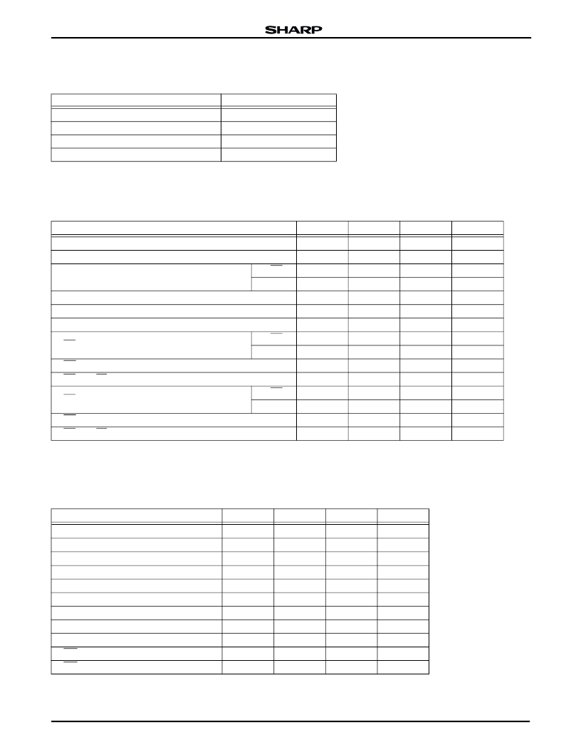
SRAM AC ELECTRICAL CHARACTERISTICS
AC Test Conditions
NOTE:
*Including scope and jig capacitance.
Read Cycle
T
A
= -25
°
C to +85
°
C, V
CC
= 2.7 V to 3.6 V
NOTE:
*Active output to HIGH impedance and HIGH impedance to output active
tests specified for a ±200 mV transition from steady state levels into the test load.
Write Cycle
T
A
= -25
°
C to +85
°
C, V
CC
= 2.7 V to 3.6 V
NOTE:
*Active output to HIGH impedance and HIGH impedance to output active
tests specified for a ±200 mV transition from steady state levels into the test load.
PARAMETER
CONDITION
Input Pulse Level
Input Rise and Fall Time
Input and Output Timing Reference Level
Output Load*
0.4 V to 2.7 V
5 ns
1.5 V
1TTL + C
L
(30 pF)
PARAMETER
SYMBOL
MIN.
MAX.
UNIT
Read Cycle Time
Address Access Time
t
RC
t
AA
t
ACE1
t
ACE2
t
BE
t
OE
t
OH
t
LZ1
t
LZ2
t
OLZ
t
BLZ
t
HZ1
t
HZ2
t
OHZ
t
BHZ
85
ns
ns
ns
ns
ns
ns
ns
ns
ns
ns
ns
ns
ns
ns
ns
85
85
85
85
45
Chip Enable Access Time
S-CE
1
S-CE
2
Byte Enable Access Time
Output Enable to Output Valid
Output hold from address change
10
10
10
10
10
0
0
0
0
S-CE
1
, S-CE
2
LOW to Output Active*
S-CE
1
S-CE
2
S-OE LOW to Output Active*
S-UB or S-LB LOW to Output in HIGH Impedance*
S-CE
1
, S-CE
2
HIGH to Output in HIGH Impedance*
S-CE
1
S-CE
2
25
25
25
25
S-OE HIGH to Output in HIGH Impedance*
S-UB or S-LB HIGH to Output in HIGH Impedance*
PARAMETER
SYMBOL
MIN.
MAX.
UNIT
Write Cycle Time
Chip Enable to End of Write
Address Valid to End of Write
Byte Enable to End of Write
Address Setup Time
Write Pulse Width
Write Recovery Time
Input Data Setup Time
Input Data Hold Time
S-WE HIGH to Output Active*
S-WE LOW to Output in HIGH Impedance*
t
WC
t
CW
t
AW
t
BW
t
AS
t
WP
t
WR
t
DW
t
DH
t
OW
t
WZ
85
75
75
75
0
65
0
35
0
5
0
ns
ns
ns
ns
ns
ns
ns
ns
ns
ns
ns
25
相關(guān)PDF資料 |
PDF描述 |
|---|---|
| LRS1805A | Stacked Chip 64M (x16) Flash Memory + 16M (x16) Smartcombo RAM |
| LRS250 | LIGHT EMITTING DIODES |
| LRS250-DO | LIGHT EMITTING DIODES |
| LRZ180-CO | Array LED 2 mm LED, Diffused |
| LS-3101S | Thyratrons |
相關(guān)代理商/技術(shù)參數(shù) |
參數(shù)描述 |
|---|---|
| LRS1342 | 制造商:Sharp Microelectronics Corporation 功能描述:COMBO 1MX16 FLASH + 128KX16 SRAM 2.7V TO 3.6V 72FBGA - Trays |
| LRS1348 | 制造商:未知廠家 制造商全稱:未知廠家 功能描述:Flash ROM |
| LRS1360 | 制造商:未知廠家 制造商全稱:未知廠家 功能描述:Flash ROM |
| LRS1360C | 制造商:未知廠家 制造商全稱:未知廠家 功能描述:MIXED MEMORY|SRAM+EEPROM|HYBRID|BGA|72PIN|PLASTIC |
| LRS1361B | 制造商:Sharp Microelectronics 功能描述:QUOTE B04419SC |
發(fā)布緊急采購,3分鐘左右您將得到回復(fù)。