- 您現(xiàn)在的位置:買賣IC網(wǎng) > PDF目錄374352 > KM29N040IT (SAMSUNG SEMICONDUCTOR CO. LTD.) 512K x 8 Bit NAND Flash Memory(512K x 8位 NAND閃速存儲器) PDF資料下載
參數(shù)資料
| 型號: | KM29N040IT |
| 廠商: | SAMSUNG SEMICONDUCTOR CO. LTD. |
| 英文描述: | 512K x 8 Bit NAND Flash Memory(512K x 8位 NAND閃速存儲器) |
| 中文描述: | 為512k × 8位NAND閃存(為512k × 8位的NAND閃速存儲器) |
| 文件頁數(shù): | 18/21頁 |
| 文件大?。?/td> | 218K |
| 代理商: | KM29N040IT |
KM29N040T, KM29N040IT
FLASH MEMORY
18
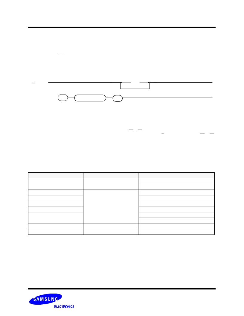
Figure 6. Block Erase Operation
BLOCK ERASE
The Erase operation is done 4K Bytes(1 block) at a time. Block address loading is accomplished in two cycles initiated by an Era se
Setup command(60H). Only address A
12
to A
18
are valid while A
8
to A
11
is ignored. The Erase Confirm command(D0H) following the
block address loading initiates the internal erasing process. This two-step sequence of setup followed by execution command
ensures that memory contents are not accidentally erased due to external noise conditions.
At the rising edge of WE after the erase confirm command input, the internal write controller handles erase, erase-verify and pulse
repetition where required.
60H
Block Add. : A
8
~A
18
I/O
0
~
7
R/B
Address Input(2Cycle)
D0H
READ STATUS
The device contains a Status Register which may be read to find out whether program or erase operation is complete, and whether
the program or erase operation completed successfully. After writing 70H command to the command register, a read cycle outputs
the contents of the Status Register to the I/O pins on the falling edge of CE or RE, whichever occurs last. This two line control allows
the system to poll the progress of each device in multiple memory connections even when R/ B pins are common-wired. RE or CE
does not need to be toggled for updated status. Refer to table 2 for specific Status Register definitions. The command register
remains in Status Read mode until further commands are issued to it. Therefore, if the status register is read during a random r ead
cycle, the required read command(00H) should be input before serial page read cycle.
SR
Status
Definition
I/O
0
Program
"0" : Successful Program
"1" : Error in Program
I/O
1
Reserved for Future Use
"0"
I/O2
"0"
I/O
3
"0"
I/O
4
"0"
I/O
5
"0"
"0"
I/O
6
Device Operation
"0" : Busy "1" : Ready
I/O
7
Write Protect
"0" : Protected "1" : Not Protected
Table2. Status Register Definition
t
BERS
相關(guān)PDF資料 |
PDF描述 |
|---|---|
| KM29N040T | 512K x 8 Bit NAND Flash Memory(512K x 8位 NAND閃速存儲器) |
| KM29N16000AIT | 2Mx8 Bit NAND Flash Memory(2Mx8位 NAND閃速存儲器) |
| KM29N16000AT | 2Mx8 Bit NAND Flash Memory(2Mx8位 NAND閃速存儲器) |
| KM29N16000ATS | 2M x 8 Bit NAND Flash Memory(2M x 8位 NAND閃速存儲器) |
| KM29N32000IT | 4M x 8 Bit NAND Flash Memory(4M x 8位 NAND閃速存儲器) |
相關(guān)代理商/技術(shù)參數(shù) |
參數(shù)描述 |
|---|---|
| KM29U128IT | 制造商:SAMSUNG 制造商全稱:Samsung semiconductor 功能描述:16M x 8 Bit NAND Flash Memory |
| KM29U128T | 制造商:SAMSUNG 制造商全稱:Samsung semiconductor 功能描述:16M x 8 Bit NAND Flash Memory |
| KM29U64000IT | 制造商:SAMSUNG 制造商全稱:Samsung semiconductor 功能描述:8M x 8 Bit NAND Flash Memory |
| KM29U64000T | 制造商:SAMSUNG 制造商全稱:Samsung semiconductor 功能描述:8M x 8 Bit NAND Flash Memory |
| KM29V16000AIT | 制造商:SAMSUNG 制造商全稱:Samsung semiconductor 功能描述:FLASH MEMORY |
發(fā)布緊急采購,3分鐘左右您將得到回復(fù)。