- 您現(xiàn)在的位置:買賣IC網(wǎng) > PDF目錄67707 > ICS950223YFLFT (INTEGRATED DEVICE TECHNOLOGY INC) 200.4 MHz, PROC SPECIFIC CLOCK GENERATOR, PDSO48 PDF資料下載
參數(shù)資料
| 型號: | ICS950223YFLFT |
| 廠商: | INTEGRATED DEVICE TECHNOLOGY INC |
| 元件分類: | 時鐘產(chǎn)生/分配 |
| 英文描述: | 200.4 MHz, PROC SPECIFIC CLOCK GENERATOR, PDSO48 |
| 封裝: | 0.300 INCH, LEAD FREE, MO-118, SSOP-48 |
| 文件頁數(shù): | 12/24頁 |
| 文件大小: | 209K |
| 代理商: | ICS950223YFLFT |
2
Integrated
Circuit
Systems, Inc.
ICS950223
0496C—05/06/05
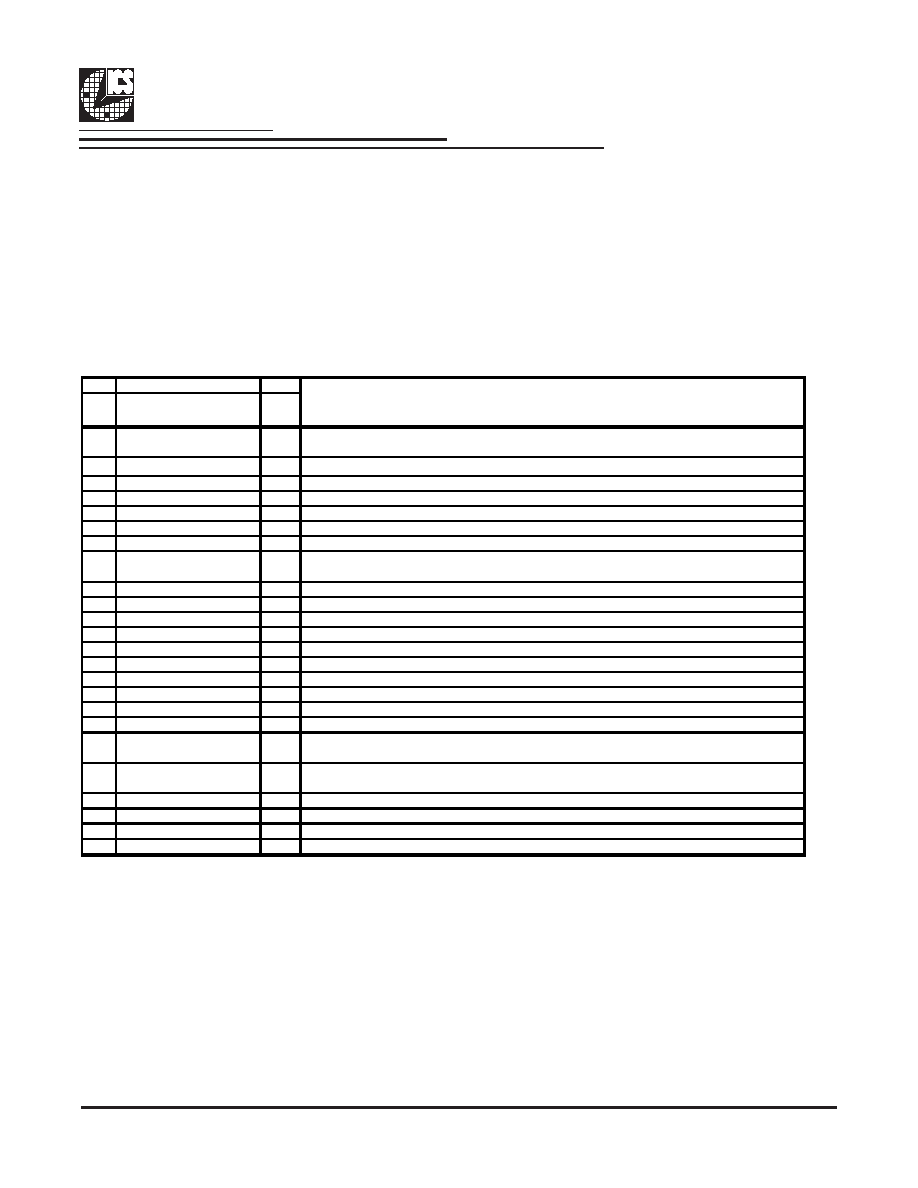
Pin Description
The ICS950223 is a single chip clock solution for desktop designs using the Intel Brookdale chipset with PC133 or DDR memory.
It provides all necessary clock signals for such a system.
The ICS950223 is part of a whole new line of ICS clock generators and buffers called TCH (Timing Control Hub). ICS is the first
to introduce a whole product line which offers full programmability and flexibility on a single clock device.This part incorporates ICS's
newest clock technology which offers more robust features and functionality. Employing the use of a serially programmable I
2C
interface, this device can adjust the output clocks by configuring the frequency setting, the output divider ratios, selecting the ideal
spread percentage, the output skew, the output strength, and enabling/disabling each individual output clock.TCH also incorporates
ICS's Watchdog Timer technology and a reset feature to provide a safe setting under unstable system conditions. M/N control can
configure output frequency with resolution up to 0.1MHz increment.With all these programmable features ICS's, TCH makes mother
board testing, tuning and improvement very simple.
General Description
PIN
#
NAME
TYPE
1
*MULTSEL1/REF1
I/O
3.3V LVTTL input for selection the current multiplier for CPU outputs / 14.318 MHz reference
clock.
2
VDDREF
PWR Ref, XTAL power supply, nominal 3.3V
3
X1
IN
Crystal input, Nominally 14.318MHz.
4
X2
OUT Crystal output, Nominally 14.318MHz
5
GND
PWR Ground pin.
6
*FS2/PCICLK0
I/O
Frequency select latch input pin / 3.3V PCI clock output.
7
*FS3/PCICLK1
I/O
Frequency select latch input pin / 3.3V PCI clock output.
8
**SEL48_24#/PCICLK2
I/O
Latched select input for 48/24MHz output. 0=24MHz, 1 = 48MHz / 3.3V PCI clock output.
9
VDDPCI
PWR Power supply for PCI clocks, nominal 3.3V
10
*FS4/PCICLK3
I/O
Frequency select latch input pin / 3.3V PCI clock output.
11
PCICLK4
OUT PCI clock output.
12
PCICLK5
OUT PCI clock output.
13
GND
PWR Ground pin.
14
PCICLK6
OUT PCI clock output.
15
PCICLK7
OUT PCI clock output.
16
PCICLK8
OUT PCI clock output.
17
PCICLK9
OUT PCI clock output.
18
VDDPCI
PWR Power supply for PCI clocks, nominal 3.3V
19
Vttpwr_GD#
IN
This 3.3V LVTTL input is a level sensitive strobe used to determine when latch inputs are
valid and are ready to be sampled. This is an active low input.
20
RESET#
OUT
Real time system reset signal for frequency gear ratio change or watchdog timer timeout.
This signal is active low.
21
GND
PWR Ground pin.
22
~*FS0/48MHz
I/O
Frequency select latch input pin / Fixed 48MHz clock output. 3.3V
23
*FS1/24_48MHz
I/O
Frequency select latch input pin / Fixed 24 or 48MHz clock output. 3.3V.
24
AVDD48
PWR Power for 24/48MHz outputs and fixed PLL core, nominal 3.3V
* Internal Pull-Up Resistor
** Internal Pull-Down Resistor
DESCRIPTION
~ This output has 2X drive
相關(guān)PDF資料 |
PDF描述 |
|---|---|
| ICS950227YFLFT | 133.33 MHz, PROC SPECIFIC CLOCK GENERATOR, PDSO56 |
| ICS950227YFT | 133.33 MHz, PROC SPECIFIC CLOCK GENERATOR, PDSO56 |
| ICS950227YFLFT | 133.33 MHz, PROC SPECIFIC CLOCK GENERATOR, PDSO56 |
| ICS950227YFT | 133.33 MHz, PROC SPECIFIC CLOCK GENERATOR, PDSO56 |
| ICS950402YFT-LF | 300 MHz, PROC SPECIFIC CLOCK GENERATOR, PDSO48 |
相關(guān)代理商/技術(shù)參數(shù) |
參數(shù)描述 |
|---|---|
| ICS950227 | 制造商:ICS 制造商全稱:ICS 功能描述:Programmable Timing Control Hub for P4 |
| ICS9502P | 制造商:未知廠家 制造商全稱:未知廠家 功能描述:Industrial Control IC |
| ICS950401 | 制造商:ICS 制造商全稱:ICS 功能描述:AMD - K8TM System Clock Chip |
| ICS950402 | 制造商:ICS 制造商全稱:ICS 功能描述:AMD - K8 System Clock Chip |
| ICS950402YFLF-T | 制造商:ICS 制造商全稱:ICS 功能描述:AMD - K8 System Clock Chip |
發(fā)布緊急采購,3分鐘左右您將得到回復(fù)。