- 您現(xiàn)在的位置:買賣IC網(wǎng) > PDF目錄296198 > HYB25D256160CC-5 (INFINEON TECHNOLOGIES AG) 256 Mbit Double Data Rate SDRAM PDF資料下載
參數(shù)資料
| 型號: | HYB25D256160CC-5 |
| 廠商: | INFINEON TECHNOLOGIES AG |
| 英文描述: | 256 Mbit Double Data Rate SDRAM |
| 中文描述: | 256兆雙倍數(shù)據(jù)速率SDRAM |
| 文件頁數(shù): | 4/94頁 |
| 文件大?。?/td> | 3326K |
| 代理商: | HYB25D256160CC-5 |
第1頁第2頁第3頁當前第4頁第5頁第6頁第7頁第8頁第9頁第10頁第11頁第12頁第13頁第14頁第15頁第16頁第17頁第18頁第19頁第20頁第21頁第22頁第23頁第24頁第25頁第26頁第27頁第28頁第29頁第30頁第31頁第32頁第33頁第34頁第35頁第36頁第37頁第38頁第39頁第40頁第41頁第42頁第43頁第44頁第45頁第46頁第47頁第48頁第49頁第50頁第51頁第52頁第53頁第54頁第55頁第56頁第57頁第58頁第59頁第60頁第61頁第62頁第63頁第64頁第65頁第66頁第67頁第68頁第69頁第70頁第71頁第72頁第73頁第74頁第75頁第76頁第77頁第78頁第79頁第80頁第81頁第82頁第83頁第84頁第85頁第86頁第87頁第88頁第89頁第90頁第91頁第92頁第93頁第94頁
HYB25D256[16/40/80]0C[E/C/F/T](L)
256 Mbit Double-Data-Rate SDRAM
Pin Configuration
Data Sheet
12
Rev. 1.6, 2004-12
2
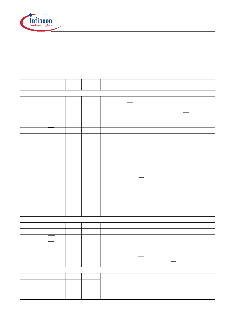
Pin Configuration
The pin configuration of a DDR SDRAM is listed by function in Table 4 (60 pins). The abbreviations used in the
Pin#/Buffer# column are explained in Table 5 and Table 6 respectively. The pin numbering for FBGA is depicted
in Figure 1 and that of the TSOP package in Figure 2
Table 4
Pin Configuration of DDR SDRAM
Ball#/Pin#
Name
Pin
Type
Buffer
Type
Function
Clock Signals
G2, 45
CK
I
SSTL
Clock Signal
Note: CK and CK are differential clock inputs. All address and
control input signals are sampled on the crossing of the
positive edge of CK and negative edge of CK. Output (read)
data is referenced to the crossings of CK and CK (both
directions of crossing).
G3, 46
CK
I
SSTL
Complementary Clock Signal
H3, 44
CKE
I
SSTL
Clock Enable Rank
Note: CKE HIGH activates, and CKE Low deactivates, internal
clock signals and device input buffers and output drivers.
Taking CKE Low provides Precharge Power-Down and Self
Refresh operation (all banks idle), or Active Power-Down
(row Active in any bank). CKE is synchronous for power
down entry and exit, and for self refresh entry. CKE is
asynchronous for self refresh exit. CKE must be maintained
high throughout read and write accesses. Input buffers,
excluding CK, CK and CKE are disabled during power-
down. Input buffers, excluding CKE, are disabled during self
refresh. CKE is an SSTL_2 input, but will detect an
LVCMOS LOW level after
V
DD is applied on first power up.
After
V
REF has become stable during the power on and
initialization sequence, it must be mantained for proper
operation of the CKE receiver. For proper self-refresh entry
and exit,
V
REF must be mantained to this input.
Control Signals
H7, 23
RAS
I
SSTL
Row Address Strobe
G8, 22
CAS
I
SSTL
Column Address Strobe
G7, 21
WE
I
SSTL
Write Enable
H8, 24
CS
I
SSTL
Chip Select
Note: All commands are masked when CS is registered HIGH. CS
provides for external bank selection on systems with
multiple banks. CS is considered part of the command code.
The standard pinout includes one CS pin.
Address Signals
J8, 26
BA0
I
SSTL
Bank Address Bus 2:0
Note: BA0 and BA1 define to which bank an Active, Read, Write
or Precharge command is being applied. BA0 and BA1 also
determines if the mode register or extended mode register
is to be accessed during a MRS or EMRS cycle.
J7, 27
BA1
I
SSTL
相關(guān)PDF資料 |
PDF描述 |
|---|---|
| HYB25S256160AC-7.5 | 16M X 16 SYNCHRONOUS DRAM, 7.5 ns, PBGA54 |
| HYB39S128160TEL-37 | MEMORY SPECTRUM |
| HYB39S128160TEL-5 | MEMORY SPECTRUM |
| HYB39S128160TEL-7 | MEMORY SPECTRUM |
| HYB39S128160TEL-75 | MEMORY SPECTRUM |
相關(guān)代理商/技術(shù)參數(shù) |
參數(shù)描述 |
|---|---|
| HYB25D256160CC-6 | 制造商:INFINEON 制造商全稱:Infineon Technologies AG 功能描述:256 Mbit Double Data Rate SDRAM |
| HYB25D256160CE-5 | 制造商:QIMONDA 制造商全稱:QIMONDA 功能描述:256-Mbit Double-Data-Rate SDRAM |
| HYB25D256160CE-5A | 制造商:QIMONDA 制造商全稱:QIMONDA 功能描述:256-Mbit Double-Data-Rate SDRAM |
| HYB25D256160CE-6 | 制造商:QIMONDA 制造商全稱:QIMONDA 功能描述:256-Mbit Double-Data-Rate SDRAM |
| HYB25D256160CEL-6 | 制造商:QIMONDA 制造商全稱:QIMONDA 功能描述:256-Mbit Double-Data-Rate SDRAM |
發(fā)布緊急采購,3分鐘左右您將得到回復。