- 您現(xiàn)在的位置:買賣IC網(wǎng) > PDF目錄371881 > HPC PDF資料下載
參數(shù)資料
| 型號(hào): | HPC |
| 文件頁(yè)數(shù): | 24/30頁(yè) |
| 文件大小: | 361K |
| 代理商: | HPC |
第1頁(yè)第2頁(yè)第3頁(yè)第4頁(yè)第5頁(yè)第6頁(yè)第7頁(yè)第8頁(yè)第9頁(yè)第10頁(yè)第11頁(yè)第12頁(yè)第13頁(yè)第14頁(yè)第15頁(yè)第16頁(yè)第17頁(yè)第18頁(yè)第19頁(yè)第20頁(yè)第21頁(yè)第22頁(yè)第23頁(yè)當(dāng)前第24頁(yè)第25頁(yè)第26頁(yè)第27頁(yè)第28頁(yè)第29頁(yè)第30頁(yè)
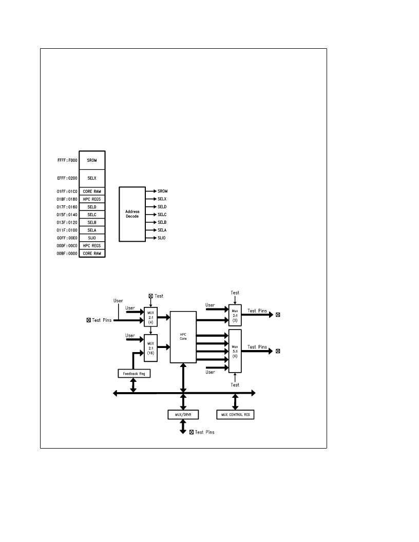
Address Decode
Address decode is a common function required when ac-
cessing memory. To aid in this function a group of 7 memory
access decode signals are available. The 64k memory map
has been divided into eleven uneven blocks. A decode sig-
nal points to a respective block of user space. The remain-
ing four blocks are accessed by internal register or RAM
memory. The latched address select bits may be used with
the required number of LSBs to decrease the amount of
circuitry necessary to decode a unique address.
Figure 19 shows the signal decode mapping. The select bit
SLIO points to a 32 byte block of memory containing Port A
registers and test registers. The remaining bytes in this
block are intended for future expansions. However, they
may be utilized as write only register locations, if desired.
TL/U/9982–21
FIGURE 19. Memory Map Partitioning
Test Logic
The HPC core contains built in test logic to aid in device
testing. This logic permits test vectors created for the stan-
dard family of products to be run while testing the Megacell
inside a cell based design. Therefore, test vector generation
to validate this complicated portion of the integrated circuit
is removed from the circuit designer. Modifications may not
be made to the test logic. Common to the strategy for all cell
based Megacells, the test logic follows the ‘‘parallel testing’’
methodology.
The parallel testing methodology isolates the core from the
remainder of the standard cell circuitry. This is accom-
plished by surrounding the core with banks of multiplexers
(see Figure 20 ). Respective multiplexer inputs and outputs
are brought to I/O pins of the device. Thus, during test the
HPC core appears as the only logic in the chip. Thirty I/O
pins are utilized by the HPC core during test. Twenty-nine of
these pins may be used for alternate functions when not in
the test mode. Sixteen pins are dedicated to Port A opera-
tion. The TEST pin determines which stimulus will reach the
core and I/O pins. This is the only I/O pin dedicated to the
test circuitry.
Two software registers assist the hardware during test. An
8-bit MUX control register (address 00FD) and a 16-bit feed-
back control register (address 00FE:00FF) are referred to
as MUXC and FDBK, respectively in the following text.
Three groups clearly define the test pins. Nine pins are out-
puts, 16 pins are bidirectional, and 5 pins are inputs. The 16
bidirectional pins are part of Port A. Port A is configured as
an address/data bus accessing the SROM address space
when in test mode. With the aid of 5:1 multiplexers and the
MUX Control register, the excessive number of outputs on
the HPC core have been brought out through 6 pins. The
outputs have been logically combined into four groups of six
outptus each. In conjunction with the TEST pin and the
MUXC register for group selection, each group is probed
separately. The ALE, NRD and NWR signals are brought out
through 2:1 MUXes.
TL/U/9982–22
FIGURE 20. HPC Core Test Logic
24
相關(guān)PDF資料 |
PDF描述 |
|---|---|
| HPE2411C | Peripheral Miscellaneous |
| HPF240D20 | |
| HPF240D30 | |
| HPF240D30R | |
| HPF240D30RS | |
相關(guān)代理商/技術(shù)參數(shù) |
參數(shù)描述 |
|---|---|
| HPC-001 | 制造商:PREMO 制造商全稱:PREMO CORPORATION S.L 功能描述:High power planar chokes for HV applications |
| HPC-002 | 制造商:PREMO 制造商全稱:PREMO CORPORATION S.L 功能描述:High power planar chokes for HV applications |
| HPC0201A0R7BXZT1 | 功能描述:硅電容器 10V 0.7pF .1pF Tol RoHS:否 制造商:IPDiA 電容:1 uF 容差:15 % 電壓額定值:5 V 溫度系數(shù):0.5 % 工作溫度范圍:- 55 C to + 150 C 封裝 / 箱體:1206 外殼高度:0.4 mm 系列:HSSC427.xxx 類型:1206 High Stability Silicon Capacitor |
| HPC0201AKIT01 | 功能描述:電容套件 SILICON RF CAP KIT 0.4-39pF RoHS:否 制造商:Nichicon 電容范圍:10 uF to 680 uF 公差范圍: 電壓范圍:6.3 V to 25 V 產(chǎn)品:Aluminum Organic Polymer Capacitor Kit |
| HPC02WE1050 | 制造商:TE Connectivity 功能描述:Labels Dot Matrix Printable Label Fabric White 50.8x5.1mm |
發(fā)布緊急采購(gòu),3分鐘左右您將得到回復(fù)。