- 您現(xiàn)在的位置:買賣IC網(wǎng) > PDF目錄371881 > HPC PDF資料下載
參數(shù)資料
| 型號(hào): | HPC |
| 文件頁(yè)數(shù): | 22/30頁(yè) |
| 文件大小: | 361K |
| 代理商: | HPC |
第1頁(yè)第2頁(yè)第3頁(yè)第4頁(yè)第5頁(yè)第6頁(yè)第7頁(yè)第8頁(yè)第9頁(yè)第10頁(yè)第11頁(yè)第12頁(yè)第13頁(yè)第14頁(yè)第15頁(yè)第16頁(yè)第17頁(yè)第18頁(yè)第19頁(yè)第20頁(yè)第21頁(yè)當(dāng)前第22頁(yè)第23頁(yè)第24頁(yè)第25頁(yè)第26頁(yè)第27頁(yè)第28頁(yè)第29頁(yè)第30頁(yè)
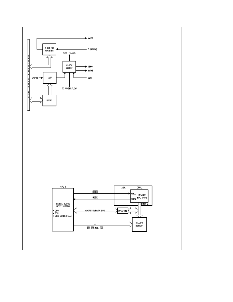
MICROWIRE/PLUS
(Continued)
TL/U/9982–19
FIGURE 17. MICROWIRE/PLUS
MICROWIRE/PLUS Operation
The HPC core can enter the MICROWIRE/PLUS mode as a
master or slave. A control bit in the IRCD register deter-
mines whether the HPC core is the master or slave mode.
An externally generated shift clock placed on the OSKI pin
is used when the HPC is configured as a slave. The OSKO
output is placed into TRI-STATE during this operation. The
shift clock is generated internally when the HPC is config-
ured as a master. The DIVBY register programs the frequen-
cy of the OSKO clock. This register allows the OSKO clock
frequency to be programmed in 14 selectable steps from
122 Hz to 1 MHz with CKI at 16.0 MHz, or from a timer T3
underflow. Hardware mode detection is provided on the MI-
CROWIRE master/slave output MWMS.
The contents of the SIO register may be accessed through
any of the memory access instructions. Data waiting to be
transmitted in the SIO register is clocked out on the falling
edge of the shift clock. Serial data on the MWIN pin is
clocked in on the rising edge of the shift clock.
Shared Memory Support
Shared memory access provides a rapid technique to ex-
change data. It is effective when data is moved from a pe-
ripheral to memory or when data is moved between blocks
of memory. A related area where shared memory access
proves effective is multiprocessing applications where two
CPUs share a common memory block. The HPC core sup-
ports shared memory access through Port A with two pins.
These pins are the NHLD input pin and the NHDA output
pin.
The host uses DMA to interface with the HPC core. A low
level on the NHLD input of the HPC core from the host
initiates a data transfer. In response, the HPC core places
Port A in a TRI-STATE mode, freeing it for use by the host.
The host waits for the acknowledge signal (NHDA) from the
HPC core indicating that the port is free. On receiving the
acknowledge, the host can rapidly transfer data into, or out
of, the shared memory by using a conventional DMA con-
troller. Upon completion of the message transfer, the host
removes the NHLD request and the HPC core resumes nor-
mal operations.
Figure 18 illustrates an application of the shared memory
interface between the HPC core and a series 32000 system.
Memory
The HPC core has been designed to offer flexibility in mem-
ory usage. A total address space of 64 kbytes can be ad-
dressed. The core contains 256 bytes of RAM, usable for
instruction execution. This 256 byte RAM block is available
as a stand alone macro for inclusion of additional memory.
Program memory addressing is controlled by the 16-bit pro-
gram counter on a byte basis. Memory can be addressed
directly by instruction or indirectly through the B, X and SP
registers. Memory can be addressed as words or bytes.
Words are always addressed on even-byte boundries. The
HPC core uses memory-mapped organization to support
registers, I/O, and on-chip peripheral functions.
The HPC core memory address space extends to 64 kbytes.
Registers and I/O are mapped as shown in Table III.
TL/U/9982–20
FIGURE 18. Shared Memory Application: HPC Core Interface to Series 32000 System
22
相關(guān)PDF資料 |
PDF描述 |
|---|---|
| HPE2411C | Peripheral Miscellaneous |
| HPF240D20 | |
| HPF240D30 | |
| HPF240D30R | |
| HPF240D30RS | |
相關(guān)代理商/技術(shù)參數(shù) |
參數(shù)描述 |
|---|---|
| HPC-001 | 制造商:PREMO 制造商全稱:PREMO CORPORATION S.L 功能描述:High power planar chokes for HV applications |
| HPC-002 | 制造商:PREMO 制造商全稱:PREMO CORPORATION S.L 功能描述:High power planar chokes for HV applications |
| HPC0201A0R7BXZT1 | 功能描述:硅電容器 10V 0.7pF .1pF Tol RoHS:否 制造商:IPDiA 電容:1 uF 容差:15 % 電壓額定值:5 V 溫度系數(shù):0.5 % 工作溫度范圍:- 55 C to + 150 C 封裝 / 箱體:1206 外殼高度:0.4 mm 系列:HSSC427.xxx 類型:1206 High Stability Silicon Capacitor |
| HPC0201AKIT01 | 功能描述:電容套件 SILICON RF CAP KIT 0.4-39pF RoHS:否 制造商:Nichicon 電容范圍:10 uF to 680 uF 公差范圍: 電壓范圍:6.3 V to 25 V 產(chǎn)品:Aluminum Organic Polymer Capacitor Kit |
| HPC02WE1050 | 制造商:TE Connectivity 功能描述:Labels Dot Matrix Printable Label Fabric White 50.8x5.1mm |
發(fā)布緊急采購(gòu),3分鐘左右您將得到回復(fù)。