- 您現(xiàn)在的位置:買賣IC網(wǎng) > PDF目錄371881 > HPC PDF資料下載
參數(shù)資料
| 型號: | HPC |
| 文件頁數(shù): | 21/30頁 |
| 文件大小: | 361K |
| 代理商: | HPC |
第1頁第2頁第3頁第4頁第5頁第6頁第7頁第8頁第9頁第10頁第11頁第12頁第13頁第14頁第15頁第16頁第17頁第18頁第19頁第20頁當(dāng)前第21頁第22頁第23頁第24頁第25頁第26頁第27頁第28頁第29頁第30頁
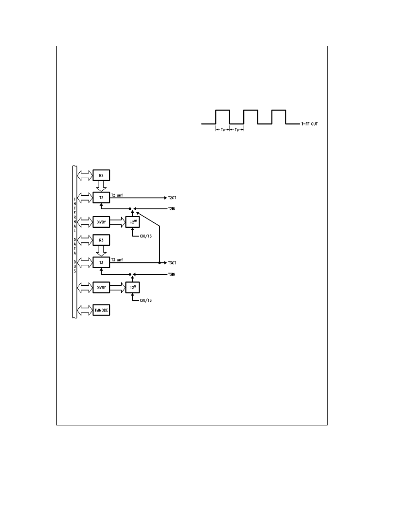
Timer Overview
(Continued)
The timers T2 and T3 have selectable clock rates. The
clock input to these two timers may be selected from the
following two sources: an external pin, T2IN and T3IN, re-
spectively, or derived internally by dividing the clock input.
Timer T2 has additional capability of being clocked by the
timer T3 underflow. This allows the user to cascade timers
T3 and T2 into a 32-bit timer/counter. The control register
DIVBY programs the clock input to timers T2 and T3 (see
Figure 15 ).
The timers T1 through T3 in conjunction with their registers
form Timer-Register pairs. The registers hold the pulse du-
ration values. All Timer-Register pairs can be read from or
written to. Each timer can be started or stopped under soft-
ware control. Once enabled, the timers count down, and
upon underflow, the contents of its associated register is
automatically loaded into the timer. An underflow on timers
T2 and T3 generates an output pulse on pins T2OT and
T3OT, respectively. The pulse is one CKI width.
TL/U/9982–17
FIGURE 15. Timers T2–T3 Block
Timer Registers
There are three control registers designated for timer pro-
gramming. The timer mode register (TMMODE) contains
control bits to start and stop timers T1 through T3. It also
contains bits to latch and enable interrupts from timers T0
through T3. The T0/capture configuration register (T0CON)
determines if (CKIN) capture registers I2CR and I3CR are to
be used as timer registers R1 and T1 or as capture regis-
ters. The divide by (DIVBY) register programs the clock in-
put to timers T2 and T3. In addition, four bits are available to
control a general purpose programmable clock brought out
on pin TDIV.
Timer Applications
The use of Pulse Width Timers for the generation of various
waveforms is easily accomplished by the HPC core.
Frequencies can be generated by using the timer/register
pairs with a toggle flip-flop. A programmable waveform may
be created by connecting the timer underflow pulse output
to the flip-flop clock. A square wave is generated when the
register value is a constant. The duty cycle can be con-
trolled simply by changing the register value.
TL/U/9982–18
FIGURE 16. Square Wave Frequency Generation
Watchdog Logic
The Watchdog Logic monitors the operations taking place
and signals upon the occurrence of any illegal activity. The
illegal conditions that trigger the Watchdog logic are poten-
tially infinite loops and illegal addresses. Should the Watch-
dog register not be written to before Timer T0 overflows
twice, or more often than once every 4096 counts of CKI/
16, an infinite loop condition is assumed to have occurred.
An illegal condition also occurs when the processor gener-
ates an illegal address. The designer specifies which ad-
dress locations are illegal through the STWD input. As well,
external logic may use the STWD input to declare a watch-
out, forcing the Watchdog logic to trigger for an illegal appli-
cation specific condition.
Any illegal condition forces the Watchdog output (WDOT)
pin high. The WDOT signal must trigger a low level on the
WDIN input for Watchdog timeout to begin. This can occur
from one of several ways. If the Watchdog feature is being
used external to the integrated circuit environment a special
watchdog I/O macro must be used. The macro has an ex-
ternal open drain output, active low. An internal output, ac-
tive low should connect back to the WDIN input on the core,
triggering a watchdog timeout. If the watchdog feature is
contained inside the IC, WDOT may be inverted and brought
back in to WDIN. The watchout signal can be connected to
the RSET or NMI interrupt input logic or be brought out for
external logic usage.
MICROWIRE/PLUS
MICROWIRE/PLUS is used for synchronous serial data
communications (see Figure 17 ). MICROWIRE/PLUS has
an 8-bit parallel-loaded, serial shift register using 15 (MWIN)
as the input and MWOT as the output. The clock signal for
the serial shift register (SIO) can be provided by an internal
or external source. The internal clock rate is programmable
by the DIVBY register and appears as a core output on
OSKO. An external clock rate may be selected on the OSKI
input of the core. Usage of OSKI or OSKO as the shift clock
is determined through the IRCD register. A DONE flag indi-
cates when the data shift is completed. The MICROWIRE/
PLUS capability enables the core to interface with any of
National Semiconductor’s MICROWIRE peripherals (i.e., A/
D converters, display drivers, EEPROMs).
21
相關(guān)PDF資料 |
PDF描述 |
|---|---|
| HPE2411C | Peripheral Miscellaneous |
| HPF240D20 | |
| HPF240D30 | |
| HPF240D30R | |
| HPF240D30RS | |
相關(guān)代理商/技術(shù)參數(shù) |
參數(shù)描述 |
|---|---|
| HPC-001 | 制造商:PREMO 制造商全稱:PREMO CORPORATION S.L 功能描述:High power planar chokes for HV applications |
| HPC-002 | 制造商:PREMO 制造商全稱:PREMO CORPORATION S.L 功能描述:High power planar chokes for HV applications |
| HPC0201A0R7BXZT1 | 功能描述:硅電容器 10V 0.7pF .1pF Tol RoHS:否 制造商:IPDiA 電容:1 uF 容差:15 % 電壓額定值:5 V 溫度系數(shù):0.5 % 工作溫度范圍:- 55 C to + 150 C 封裝 / 箱體:1206 外殼高度:0.4 mm 系列:HSSC427.xxx 類型:1206 High Stability Silicon Capacitor |
| HPC0201AKIT01 | 功能描述:電容套件 SILICON RF CAP KIT 0.4-39pF RoHS:否 制造商:Nichicon 電容范圍:10 uF to 680 uF 公差范圍: 電壓范圍:6.3 V to 25 V 產(chǎn)品:Aluminum Organic Polymer Capacitor Kit |
| HPC02WE1050 | 制造商:TE Connectivity 功能描述:Labels Dot Matrix Printable Label Fabric White 50.8x5.1mm |
發(fā)布緊急采購,3分鐘左右您將得到回復(fù)。