- 您現在的位置:買賣IC網 > PDF目錄67505 > FMS9874AKGC100 (FAIRCHILD SEMICONDUCTOR CORP) 3-CH 8-BIT PROPRIETARY METHOD ADC, PARALLEL ACCESS, PQFP100 PDF資料下載
參數資料
| 型號: | FMS9874AKGC100 |
| 廠商: | FAIRCHILD SEMICONDUCTOR CORP |
| 元件分類: | ADC |
| 英文描述: | 3-CH 8-BIT PROPRIETARY METHOD ADC, PARALLEL ACCESS, PQFP100 |
| 封裝: | MQFP-100 |
| 文件頁數: | 2/26頁 |
| 文件大小: | 454K |
| 代理商: | FMS9874AKGC100 |
PRODUCT SPECIFICATION
FMS9874A
10
REV. 1.2.10 1/14/02
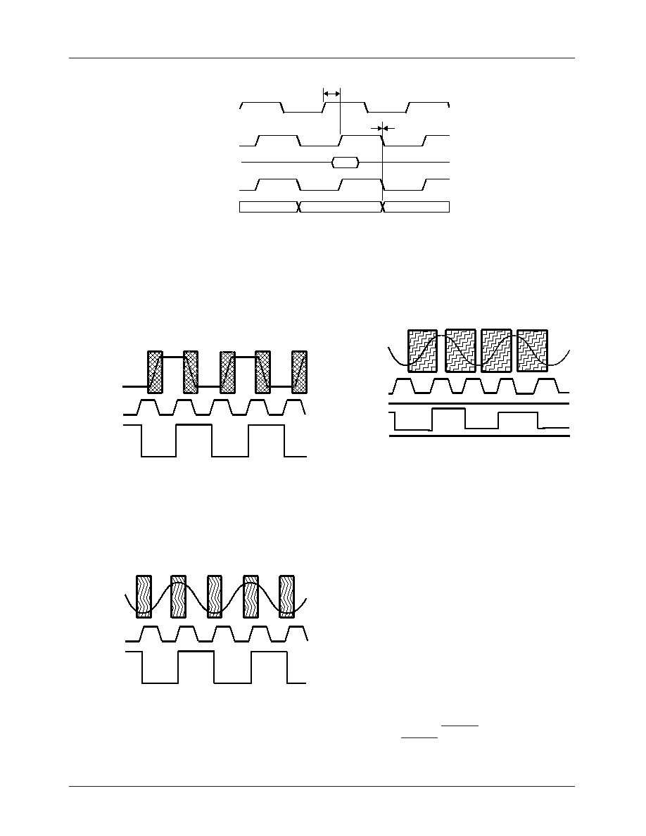
Ideally, incoming pixels (PC generated) would be trapezoi-
dal with fast rise-times and the sampling edge of the A/D
clock, SCK would be positioned along the level section of
the incoming pixel waveform as shown in Figure 4. There is
a narrow zone of uncertainly where sampling during pixel
rise time would cause an error in the value of the A/D data
output, D7-0, which is shown as a value, 0-255.
Figure 4. Ideal Pixel Sampling
In practice, high-resolution pixels have relatively long rise-
times. As shown in Figure 5, there are narrow zones of seren-
dipity when the pixel amplitude is level. Samples are valid in
these zones.
Figure 5. Acceptable Pixel Sampling
Referring to Figure 6, when the sample clock, SCK has some
jitter, if the sampling edge occurs anywhere within the zone
of uncertainty where the pixel rise time is steep, there will be
amplitude modulation of the digitized data, D7-0, due to the
sampling clock jitter. To avoid corruption of the image, set-
ting the value PHASE7-0 is critical. PHASE4-0 should be
trimmed to position the sampling edge of SCK within the
zone of serendipity.
Figure 6. Improper Pixel Sampling
Voltage References
An on-chip voltage reference is generated from a bandgap
source. VREFOUT is the buffered output of this source that
can be connected to VREFIN to supply a voltage reference
that is common to the three converter channels.
VREFIN, with a nominal voltage of 1.25V, is the source of the
differential reference voltages for each A/D converter.
Reference voltages supplied to the differential inputs of the
comparators in the A/D converters are derived from VREFIN.
Digital Data Outputs
Input horizontal sync HSIN and outgoing data, D[7..0] are
resynchronized to the delayed sample clock, SCK. Output
timing relationships are dened in Figure 7. Latency of the
rst pixel, N varies according to the mode:
1.
Normal.
2.
Alternate pixel sampling.
Levels are 3.3 volt CMOS. PWRDN = L sets the outputs
high-impedance. PWRDN = H enables the outputs.
D7-0
RIN, GIN, BIN
SCK
Zones of Uncertainty
D7-0
RIN, GIN, BIN
SCK
Zones of Serendipity
D7-0
RIN, GIN, BIN
SCK
Zones of Uncertainty
Figure 3. Internal Sampling Clock, SCK Timing
PHASE
Sn
PXCK/XCK
SCK
VIN
DCK
DA
相關PDF資料 |
PDF描述 |
|---|---|
| FMS9874AKGC140 | 3-CH 8-BIT PROPRIETARY METHOD ADC, PARALLEL ACCESS, PQFP100 |
| FMS9875KGC100 | 3-CH 8-BIT PROPRIETARY METHOD ADC, PARALLEL ACCESS, PQFP100 |
| FMS9875KGC100X | 3-CH 8-BIT PROPRIETARY METHOD ADC, PARALLEL ACCESS, PQFP100 |
| FMS9875KGC140 | 3-CH 8-BIT PROPRIETARY METHOD ADC, PARALLEL ACCESS, PQFP100 |
| FMS9875KGC140X | 3-CH 8-BIT PROPRIETARY METHOD ADC, PARALLEL ACCESS, PQFP100 |
相關代理商/技術參數 |
參數描述 |
|---|---|
| FMS9874KGC | 功能描述:視頻 IC RoHS:否 制造商:Fairchild Semiconductor 工作電源電壓:5 V 電源電流:80 mA 最大工作溫度:+ 85 C 封裝 / 箱體:TSSOP-28 封裝:Reel |
| FMS9874KGC100 | 制造商:FAIRCHILD 制造商全稱:Fairchild Semiconductor 功能描述:Graphics Digitizer - 3x8-Bit, 108Ms/s Triple Video A/D Converter with Clamps |
| FMS9875 | 制造商:FAIRCHILD 制造商全稱:Fairchild Semiconductor 功能描述:Triple 8-Bit, 108/140 MHz A/D Converter with Clamps and PLL |
| FMS9875KAC100 | 制造商:FAIRCHILD 制造商全稱:Fairchild Semiconductor 功能描述:Triple 8-Bit, 108/140 MHz A/D Converter with Clamps and PLL |
| FMS9875KAC140 | 制造商:FAIRCHILD 制造商全稱:Fairchild Semiconductor 功能描述:Triple 8-Bit, 108/140 MHz A/D Converter with Clamps and PLL |
發(fā)布緊急采購,3分鐘左右您將得到回復。