- 您現(xiàn)在的位置:買賣IC網(wǎng) > PDF目錄362685 > EM78569 (ELAN Microelctronics Corp .) 8-BIT MICRO-CONTROLLER PDF資料下載
參數(shù)資料
| 型號: | EM78569 |
| 廠商: | ELAN Microelctronics Corp . |
| 英文描述: | 8-BIT MICRO-CONTROLLER |
| 中文描述: | 8位微控制器 |
| 文件頁數(shù): | 48/53頁 |
| 文件大小: | 461K |
| 代理商: | EM78569 |
第1頁第2頁第3頁第4頁第5頁第6頁第7頁第8頁第9頁第10頁第11頁第12頁第13頁第14頁第15頁第16頁第17頁第18頁第19頁第20頁第21頁第22頁第23頁第24頁第25頁第26頁第27頁第28頁第29頁第30頁第31頁第32頁第33頁第34頁第35頁第36頁第37頁第38頁第39頁第40頁第41頁第42頁第43頁第44頁第45頁第46頁第47頁當前第48頁第49頁第50頁第51頁第52頁第53頁
EM78569
8-bit Micro-controller
__________________________________________________________________________________________________________________________________________________________________
* This specification is subject to be changed without notice.
8/31/2004 (V4.0)
Fosc: Input clock.
Prescaler ( T1P0 and T1P1/T2P1 and T2P0 ): Options of 1:2, 1:8, 1:32, and 1:64 are defined by TMRX. It is
cleared when any type of reset occurs.
TMR1X and TMR2X (TMR1H/TWR1L and TMR2H/TMR2L ):Timer X register; TMRX is increased until
it matches with PRDX, and then is reset to 0. TMRX cannot be read.
PRDX ( PRD1 and PRD2 ): PWM period register.
When defining TMRX, refer to the related registers of its operation as shown in prescale register. It must be
noted that the PWMX bits must be disabled if their related TMRXs are employed. That is, bit 7 and bit 6 of
the PWMCON register must be set to ‘0’.
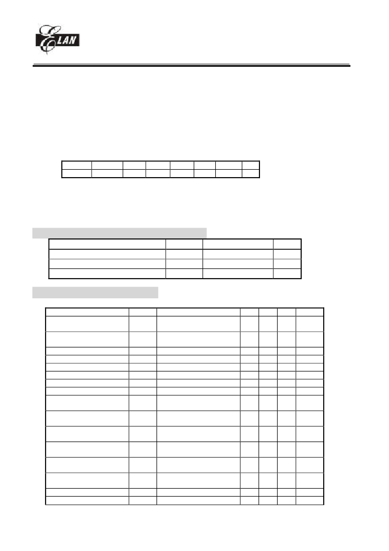
Related Control Registers(R5 PAGE3) of TMR1 and TMR2
Bit 7
Bit 6
Bit 5
PWM2E
PWM1E
T2EN
Bit 4
T1EN
Bit 3
T2P1
Bit 2
T2P0
Bit 1
T1P1
Bit 0
T1P0
Timer programming procedures/steps
(1) Load PRDX with the TIMER period.
(2) Enable interrupt function by writing IOCF PAGE0, if required
(3) Load a desired value to PWMCON with the TMRX prescaler value and enable both TMRX and disable
PWMX.
VIII. Absolute Operation Maximum Ratings
RATING
DC SUPPLY VOLTAGE
INPUT VOLTAGE
OPERATING TEMPERATURE RANGE
SYMBOL
VDD
Vin
Ta
VALUE
-0.3 To 6
-0.5 to VDD +0.5
0 to 70
UNIT
V
V
IX. DC Electrical Characteristic
(Ta = 25
°
C, VDD=5V
±
5%, VSS=0V)
Parameter
Input leakage current for
input pins
Input leakage current for bi-
directional pins
Input high voltage
Input low voltage
Input high threshold voltage
Input low threshold voltage
Clock input high voltage
Clock input low voltage
Output high voltage for
PORT5,B,C,
Output high voltage for
PORT6,7,8
Output high voltage for
PORT9
Output low voltage for
PORT5,B,C
Output low voltage for
PORT6,7,8
Output low voltage for
PORT9
LCD drive reference voltage
Pull-high current
Symbol Condition
IIL1
VIN = VDD, VSS
Min
Typ
Max
±
1
Unit
μ
A
IIL2
VIN = VDD, VSS
±
1
μ
A
VIH
VIL
VIHT
VILT
VIHX
VILX
VOH1
/RESET, TCC
/RESET, TCC
OSCI
OSCI
IOH = -6mA
2.5
V
V
V
V
V
V
V
0.8
0.8
1.5
2.0
3.5
2.4
VOH2
IOH = -12mA
2.4
V
VOH3
IOH = -15mA
2.4
V
VOL1
IOH = 6mA
0.4
V
VOL2
IOH = 12mA
0.4
V
VOL3
IOH = 15mA
0.4
V
VLCD
IPH
VDD=5V, Contrast adjust
Pull-high active input pin at
4 ~ 5
-10
V
μ
A
-15
相關PDF資料 |
PDF描述 |
|---|---|
| EM785830AA | 8-BIT MICRO-CONTROLLER |
| EM785830AAM | 8-BIT MICRO-CONTROLLER |
| EM785830AAP | 8-BIT MICRO-CONTROLLER |
| EM785830AD | 8-BIT MICRO-CONTROLLER |
| EM785830ADQ | 8-BIT MICRO-CONTROLLER |
相關代理商/技術參數(shù) |
參數(shù)描述 |
|---|---|
| EM785830AA | 制造商:EMC 制造商全稱:ELAN Microelectronics Corp 功能描述:8-BIT MICRO-CONTROLLER |
| EM785830AAM | 制造商:EMC 制造商全稱:ELAN Microelectronics Corp 功能描述:8-BIT MICRO-CONTROLLER |
| EM785830AAP | 制造商:EMC 制造商全稱:ELAN Microelectronics Corp 功能描述:8-BIT MICRO-CONTROLLER |
| EM785830AD | 制造商:EMC 制造商全稱:ELAN Microelectronics Corp 功能描述:8-BIT MICRO-CONTROLLER |
| EM785830ADQ | 制造商:EMC 制造商全稱:ELAN Microelectronics Corp 功能描述:8-BIT MICRO-CONTROLLER |
發(fā)布緊急采購,3分鐘左右您將得到回復。