- 您現(xiàn)在的位置:買賣IC網(wǎng) > PDF目錄171235 > DSRT-L030-011 (CONEXANT SYSTEMS) SPECIALTY CONSUMER CIRCUIT, XMA PDF資料下載
參數(shù)資料
| 型號: | DSRT-L030-011 |
| 廠商: | CONEXANT SYSTEMS |
| 元件分類: | 消費家電 |
| 英文描述: | SPECIALTY CONSUMER CIRCUIT, XMA |
| 文件頁數(shù): | 16/86頁 |
| 文件大?。?/td> | 667K |
| 代理商: | DSRT-L030-011 |
第1頁第2頁第3頁第4頁第5頁第6頁第7頁第8頁第9頁第10頁第11頁第12頁第13頁第14頁第15頁當(dāng)前第16頁第17頁第18頁第19頁第20頁第21頁第22頁第23頁第24頁第25頁第26頁第27頁第28頁第29頁第30頁第31頁第32頁第33頁第34頁第35頁第36頁第37頁第38頁第39頁第40頁第41頁第42頁第43頁第44頁第45頁第46頁第47頁第48頁第49頁第50頁第51頁第52頁第53頁第54頁第55頁第56頁第57頁第58頁第59頁第60頁第61頁第62頁第63頁第64頁第65頁第66頁第67頁第68頁第69頁第70頁第71頁第72頁第73頁第74頁第75頁第76頁第77頁第78頁第79頁第80頁第81頁第82頁第83頁第84頁第85頁第86頁
RipTide PCI Audio/Comm Device Family Product Description
1167
ROCKWELL PROPRIETARY INFORMATION
23
4.3.4
AC Electrical Characteristics
4.3.4.1
PCI Interface Signals
The PCI interface timing for PCI interface signals (4.2.1) conforms to the PCI Local Bus Specification, Production Version,
Revision 2.1, June 1, 1995.
4.3.4.2
PnP Serial EEPROM Interface Signals
An external 1K bit (64 x 16) PnP serial EEPROM is required only if the product and manufacturers ID for Plug and Play is to
be modified to other than the Rockwell registered IDs. Otherwise, the internal ROM can be used for PnP support to reduce
manufacturing cost. If the EEPROM is not used, specific discrete components must be depopulated (refer to the RipTide
reference design schematic).
The serial EEPROM interface meets the timing requirements of an Atmel AT93C46, Microchip Technology, Inc. 93LC46B, or
equivalent 1K bit (64 x 16) device. Note: Atmel AT93C46 is used, connect pin 6 of the AT93C46 to VCC to select x16
configuration.
The following summarizes timing information for serial EEPROM interface signals.
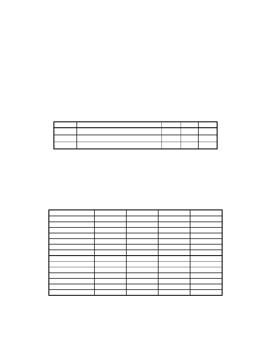
Symbol
Parameter
Min
Max
Units
tval
CLK to Signal Valid Delay
400
ns
tsu
Input Set-up Time to CLK
100
ns
th
Input Hold Time from CLK
100
ns
4.3.4.3
Codec AC-link Interface Signals
The AC-link timing is described in Section 5.4.5.
4.3.4.4
JTAG Interface
When enabled, the JTAG interface uses the TCK input as its clock. All pins of the device have JTAG implemented. Please
refer to IEEE Std 1149.1 for timing information.
4.3.4.5
Modem DSP Parallel Host Bus Interface
Parameter
Symbol
Min.
Max.
Units
a. Read
Address Setup
TRS
10
–
ns
Chip Select Setup
TCS
0
–
ns
Control Hold
THC
10
–
ns
Read Data Access
TDA
-
35
ns
Read Data Hold
TDHR
10
–
ns
Read Pulse Width
TRR
45
–
ns
b. Write
Address Setup
TRS
10
–
ns
Chip Select Setup
TCS
0
–
ns
Control Hold
THC
10
–
ns
Write Data Setup
TWDS
10
–
ns
Write Data Hold
TWDH
10
–
ns
Write Pulse Width
TWW
45
–
ns
相關(guān)PDF資料 |
PDF描述 |
|---|---|
| DSRT-L050-011 | SPECIALTY CONSUMER CIRCUIT, XMA |
| DSS710D223S12-22 | 1 FUNCTIONS, 12 V, 7 A, DATA LINE FILTER |
| DST9HB32E101Q55J | 1 FUNCTIONS, 250 V, 6 A, DATA LINE FILTER |
| DST9HB32E220Q55J | 1 FUNCTIONS, 250 V, 6 A, DATA LINE FILTER |
| DST9HB32E222Q55J | 1 FUNCTIONS, 250 V, 6 A, DATA LINE FILTER |
相關(guān)代理商/技術(shù)參數(shù) |
參數(shù)描述 |
|---|---|
| DSR-TSS-S1 | 制造商:DOMINANT 制造商全稱:DOMINANT Semiconductors 功能描述:Right Angle LED |
| DSR-TSS-S2 | 制造商:DOMINANT 制造商全稱:DOMINANT Semiconductors 功能描述:Right Angle LED |
| DSR-TSS-ST2-1 | 制造商:DOMINANT 制造商全稱:DOMINANT Semiconductors 功能描述:Right Angle LED |
| DSR-TSS-T1 | 制造商:DOMINANT 制造商全稱:DOMINANT Semiconductors 功能描述:Right Angle LED |
| DSR-TSS-T2 | 制造商:DOMINANT 制造商全稱:DOMINANT Semiconductors 功能描述:Right Angle LED |
發(fā)布緊急采購,3分鐘左右您將得到回復(fù)。