- 您現(xiàn)在的位置:買賣IC網(wǎng) > PDF目錄378593 > DSP56800ERM (飛思卡爾半導(dǎo)體(中國)有限公司) 16-bit Digital Signal Controllers PDF資料下載
參數(shù)資料
| 型號: | DSP56800ERM |
| 廠商: | 飛思卡爾半導(dǎo)體(中國)有限公司 |
| 英文描述: | 16-bit Digital Signal Controllers |
| 中文描述: | 16位數(shù)字信號控制器 |
| 文件頁數(shù): | 17/124頁 |
| 文件大小: | 1880K |
| 代理商: | DSP56800ERM |
第1頁第2頁第3頁第4頁第5頁第6頁第7頁第8頁第9頁第10頁第11頁第12頁第13頁第14頁第15頁第16頁當(dāng)前第17頁第18頁第19頁第20頁第21頁第22頁第23頁第24頁第25頁第26頁第27頁第28頁第29頁第30頁第31頁第32頁第33頁第34頁第35頁第36頁第37頁第38頁第39頁第40頁第41頁第42頁第43頁第44頁第45頁第46頁第47頁第48頁第49頁第50頁第51頁第52頁第53頁第54頁第55頁第56頁第57頁第58頁第59頁第60頁第61頁第62頁第63頁第64頁第65頁第66頁第67頁第68頁第69頁第70頁第71頁第72頁第73頁第74頁第75頁第76頁第77頁第78頁第79頁第80頁第81頁第82頁第83頁第84頁第85頁第86頁第87頁第88頁第89頁第90頁第91頁第92頁第93頁第94頁第95頁第96頁第97頁第98頁第99頁第100頁第101頁第102頁第103頁第104頁第105頁第106頁第107頁第108頁第109頁第110頁第111頁第112頁第113頁第114頁第115頁第116頁第117頁第118頁第119頁第120頁第121頁第122頁第123頁第124頁
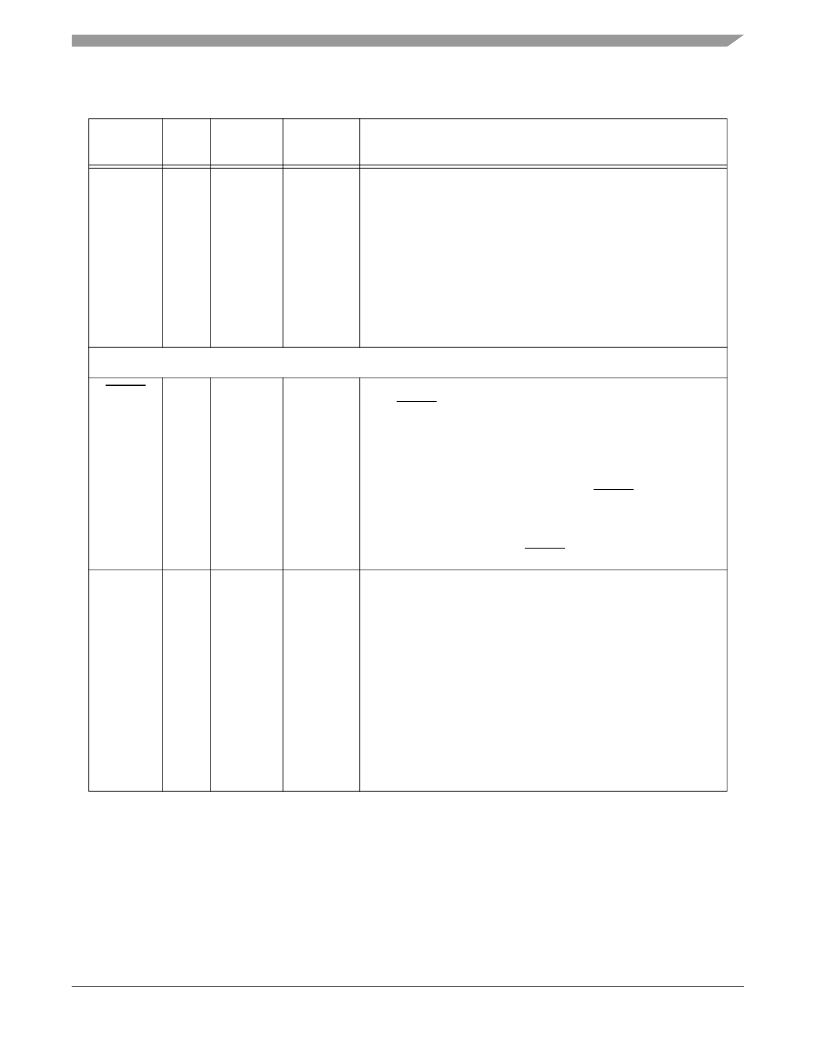
56F8013 Signal Pins
56F8013 Technical Data, Rev. 2
Freescale Semiconductor
Preliminary
17
GPIOB7
(TXD)
(SCL
2
)
3
Input/
Output
Input/
Output
Input/
Output
Input, pulled
high
internally
Port B GPIO
— This GPIO pin can be individually programmed as
an input or output pin.
Transmit Data
— SCI transmit data output or transmit / receive in
single wire operation.
Serial Clock
— This pin serves as the I
2
C serial clock.
After reset, the default state is GPIOB7. The peripheral functionality
is controlled via the SIM. See
Section 6.3.8
.
2.
This signal is also brought out on the GPIOB0 pin.
RESET
(GPIOA7)
15
Input
Input/Open
Drain
Output
Input, pulled
high
internally
Reset
— This input is a direct hardware reset on the processor.
When RESET is asserted low, the chip is initialized and placed in the
reset state. A Schmitt trigger input is used for noise immunity. The
internal reset signal will be deasserted synchronous with the internal
clocks after a fixed number of internal clocks.
Port A GPIO
— This GPIO pin can be individually programmed as
an input or open drain output pin. Note that RESET functionality is
disabled in this mode and the chip can only be reset via POR, COP
reset, or software reset.
After reset, the default state is RESET.
GPIOB4
(T0)
(CLKO)
19
Input/
Output
Input/
Output
Output
Input, pulled
high
internally
Port B GPIO
— This GPIO pin can be individually programmed as
an input or output pin.
T0
— Timer, Channel 0
Clock Output
— This is a buffered clock signal. Using the
SIM_CLKO Select Register (SIM_CLKOSR), this pin can be
programmed as any of the following: disabled (logic 0), CLK_MSTR
(system clock), IPBus clock, or oscillator output. See
Section 6.3.7
.
After reset, the default state is GPIOB4. The peripheral functionality
is controlled via the SIM. See
Section 6.3.8
.
Return to
Table 2-2
Table 2-3 56F8013 Signal and Package Information for the 32-Pin LQFP (Continued)
Signal
Name
LQFP
Pin No.
Type
State During
Reset
Signal Description
相關(guān)PDF資料 |
PDF描述 |
|---|---|
| DSP56800E | Digitial Signal Controller |
| DSP56853 | Digitial Signal Controller |
| DSP56854 | Digitial Signal Controller |
| DSP56855 | Digitial Signal Controller |
| DSP56856 | Digitial Signal Controller |
相關(guān)代理商/技術(shù)參數(shù) |
參數(shù)描述 |
|---|---|
| DSP56800ESDKPB | 制造商:未知廠家 制造商全稱:未知廠家 功能描述:Embedded SDK for DSP56800E Rev 2.0E. Rev 6.0 Product Brief |
| DSP56800FM | 制造商:MOTOROLA 制造商全稱:Motorola, Inc 功能描述:Preliminary Technical Data DSP56F826 16-bit Digital Signal Processor |
| DSP56800FM/D | 制造商:MOTOROLA 制造商全稱:Motorola, Inc 功能描述:DSP56824 16-Bit Digital Signal Processor |
| DSP56800FMD | 制造商:MOTOROLA 制造商全稱:Motorola, Inc 功能描述:Preliminary Technical Data DSP56F826 16-bit Digital Signal Processor |
| DSP56800SDKPB | 制造商:未知廠家 制造商全稱:未知廠家 功能描述:Embedded SDK for DSP56800 Rev 3.0. Rev 7.0 Product Brief |
發(fā)布緊急采購,3分鐘左右您將得到回復(fù)。