- 您現(xiàn)在的位置:買(mǎi)賣(mài)IC網(wǎng) > PDF目錄377000 > DSP56321VL240 (飛思卡爾半導(dǎo)體(中國(guó))有限公司) 24-Bit Digital Signal Processor PDF資料下載
參數(shù)資料
| 型號(hào): | DSP56321VL240 |
| 廠商: | 飛思卡爾半導(dǎo)體(中國(guó))有限公司 |
| 元件分類(lèi): | 數(shù)字信號(hào)處理 |
| 英文描述: | 24-Bit Digital Signal Processor |
| 中文描述: | 24位數(shù)字信號(hào)處理器 |
| 文件頁(yè)數(shù): | 44/84頁(yè) |
| 文件大小: | 898K |
| 代理商: | DSP56321VL240 |
第1頁(yè)第2頁(yè)第3頁(yè)第4頁(yè)第5頁(yè)第6頁(yè)第7頁(yè)第8頁(yè)第9頁(yè)第10頁(yè)第11頁(yè)第12頁(yè)第13頁(yè)第14頁(yè)第15頁(yè)第16頁(yè)第17頁(yè)第18頁(yè)第19頁(yè)第20頁(yè)第21頁(yè)第22頁(yè)第23頁(yè)第24頁(yè)第25頁(yè)第26頁(yè)第27頁(yè)第28頁(yè)第29頁(yè)第30頁(yè)第31頁(yè)第32頁(yè)第33頁(yè)第34頁(yè)第35頁(yè)第36頁(yè)第37頁(yè)第38頁(yè)第39頁(yè)第40頁(yè)第41頁(yè)第42頁(yè)第43頁(yè)當(dāng)前第44頁(yè)第45頁(yè)第46頁(yè)第47頁(yè)第48頁(yè)第49頁(yè)第50頁(yè)第51頁(yè)第52頁(yè)第53頁(yè)第54頁(yè)第55頁(yè)第56頁(yè)第57頁(yè)第58頁(yè)第59頁(yè)第60頁(yè)第61頁(yè)第62頁(yè)第63頁(yè)第64頁(yè)第65頁(yè)第66頁(yè)第67頁(yè)第68頁(yè)第69頁(yè)第70頁(yè)第71頁(yè)第72頁(yè)第73頁(yè)第74頁(yè)第75頁(yè)第76頁(yè)第77頁(yè)第78頁(yè)第79頁(yè)第80頁(yè)第81頁(yè)第82頁(yè)第83頁(yè)第84頁(yè)
DSP56321 Technical Data, Rev. 11
2-24
Freescale Semiconductor
Specifications
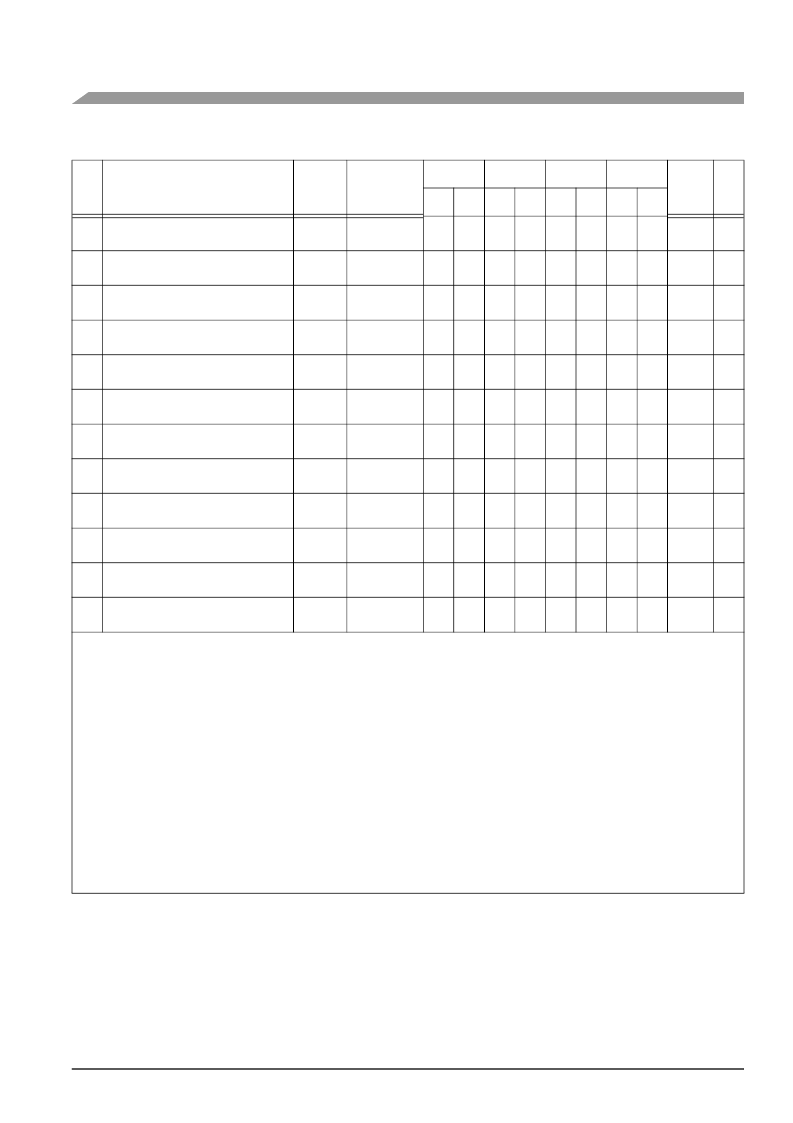
451 TXC rising edge to FST out (word-
length) low
—
—
12.5
8.3
—
—
12.5
8.3
—
—
12.5
8.3
—
—
12.5
8.3
x ck
i ck
ns
452 TXC rising edge to data out enable from
high impedance
—
—
12.5
8.3
—
—
12.5
8.3
—
—
12.5
8.3
—
—
12.5
8.3
x ck
i ck
ns
453 TXC rising edge to Transmitter 0 drive
enable assertion
—
—
12.5
13.5
—
—
12.5
13.5
—
—
12.5
13.5
—
—
12.5
13.5
x ck
i ck
ns
454 TXC rising edge to data out valid
—
—
12.5
8.3
—
—
12.5
8.3
—
—
12.5
8.3
—
—
12.5
8.3
x ck
i ck
ns
455 TXC rising edge to data out high
impedance
3
—
—
30.0
8.3
—
—
30.0
8.3
—
—
30.0
8.3
—
—
30.0
8.3
x ck
i ck
ns
456 TXC rising edge to Transmitter 0 drive
enable deassertion
3
—
—
12.5
8.3
—
—
12.5
8.3
—
—
12.5
8.3
—
—
12.5
8.3
x ck
i ck
ns
457 FST input (bl, wr) setup time before
TXC falling edge
2
5.0
10.0
—
—
5.0
10.0
—
—
5.0
10.0
—
—
5.0
10.0
—
—
x ck
i ck
ns
458 FST input (wl) to data out enable from
high impedance
—
—
15.0
8.0
—
—
15.0
8.0
—
—
15.0
8.0
—
—
15.0
8.0
x ck
i ck
ns
459 FST input (wl) to Transmitter 0 drive
enable assertion
—
—
15.0
18.0
—
—
15.0
18.0
—
—
15.0
18.0
—
—
15.0
18.0
x ck
i ck
ns
460 FST input (wl) setup time before TXC
falling edge
5.0
10.0
—
—
5.0
10.0
—
—
5.0
10.0
—
—
5.0
10.0
—
—
x ck
i ck
ns
461 FST input hold time after TXC falling
edge
3.8
5.0
—
—
3.8
5.0
—
—
3.8
5.0
—
—
3.8
5.0
—
—
x ck
i ck
ns
462 Flag output valid after TXC rising edge
—
—
12.5
8.3
—
—
12.5
8.3
—
—
12.5
8.3
—
—
12.5
8.3
x ck
i ck
ns
Notes:
1.
For the internal clock, the external clock cycle is defined by the instruction cycle time (timing 7 in
Table 2-5
on page 2-4) and the
ESSI control register. T
ECCX
must be
≥
T
C
×
3, in accordance with the note below Table 7-1 in the DSP56321 Reference
Manual. T
ECCI
must be
≥
T
C
×
4, in accordance with the explanation of CRA[PSR] and the ESSI Clock Generator Functional
Block Diagram shown in
Figure 7-3
of the DSP56321 Reference Manual.
The word-length-relative frame sync signal waveform operates the same way as the bit-length frame sync signal waveform, but
spreads from one serial clock before the first bit clock (same as the Bit Length Frame Sync signal) until the one before last bit
clock of the first word in the frame.
Periodically sampled and not 100 percent tested
V
CCQH
= 3.3 V
±
0.3 V, V
CCQL
= 1.6 V
±
0.1 V; T
J
=
0°C to +85°C, C
L
= 50 pF
TXC (SCK Pin) = Transmit Clock
RXC (SC0 or SCK Pin) = Receive Clock
FST (SC2 Pin) = Transmit Frame Sync
FSR (SC1 or SC2 Pin) Receive Frame Sync
i ck = Internal Clock; x ck = External Clock
i ck a = Internal Clock, Asynchronous Mode (asynchronous implies that TXC and RXC are two different clocks)
i ck s = Internal Clock, Synchronous Mode (synchronous implies that TXC and RXC are the same clock)
In the timing diagrams below, the clocks and frame sync signals are drawn using the clock falling edge as a the first reference.
Clock and frame sync polarities are programmable in Control Register B (CRB). Refer to the DSP56321 Reference Manualfor
details.
2.
3.
4.
5.
6.
7.
Table 2-12.
ESSI Timings (Continued)
No.
Characteristics
4, 6
Symbol
Expression
200 MHz
220 MHz
240 MHz
275 MHz
Cond-
ition
5
Unit
Min Max Min Max Min Max Min Max
相關(guān)PDF資料 |
PDF描述 |
|---|---|
| DSP56321VL275 | 24-Bit Digital Signal Processor |
| DSP56364P | 24-Bit Audio Digital Signal Processor |
| DSP56366P | 24-Bit Audio Digital Signal Processor |
| DSP56366UM | 24-Bit Audio Digital Signal Processor |
| DSP56367P | 24-Bit Audio Digital Signal Processor |
相關(guān)代理商/技術(shù)參數(shù) |
參數(shù)描述 |
|---|---|
| DSP56321VL275 | 功能描述:數(shù)字信號(hào)處理器和控制器 - DSP, DSC 24 BIT DSP PBFREE RoHS:否 制造商:Microchip Technology 核心:dsPIC 數(shù)據(jù)總線寬度:16 bit 程序存儲(chǔ)器大小:16 KB 數(shù)據(jù) RAM 大小:2 KB 最大時(shí)鐘頻率:40 MHz 可編程輸入/輸出端數(shù)量:35 定時(shí)器數(shù)量:3 設(shè)備每秒兆指令數(shù):50 MIPs 工作電源電壓:3.3 V 最大工作溫度:+ 85 C 封裝 / 箱體:TQFP-44 安裝風(fēng)格:SMD/SMT |
| DSP56321VL275 | 制造商:Freescale Semiconductor 功能描述:Digital Signal Processor (DSP) IC |
| DSP56362 | 制造商:FREESCALE 制造商全稱(chēng):Freescale Semiconductor, Inc 功能描述:24-Bit Audio Digital Signal Processor |
| DSP56362AD | 制造商:MOTOROLA 制造商全稱(chēng):Motorola, Inc 功能描述:24-Bit Audio Digital Signal Processor |
| DSP56362D | 制造商:MOTOROLA 制造商全稱(chēng):Motorola, Inc 功能描述:24-Bit Audio Digital Signal Processor |
發(fā)布緊急采購(gòu),3分鐘左右您將得到回復(fù)。