- 您現(xiàn)在的位置:買賣IC網(wǎng) > PDF目錄369679 > CYNSE70128 Network Processing PDF資料下載
參數(shù)資料
| 型號(hào): | CYNSE70128 |
| 英文描述: | Network Processing |
| 中文描述: | 網(wǎng)絡(luò)處理 |
| 文件頁(yè)數(shù): | 98/126頁(yè) |
| 文件大小: | 3302K |
| 代理商: | CYNSE70128 |
第1頁(yè)第2頁(yè)第3頁(yè)第4頁(yè)第5頁(yè)第6頁(yè)第7頁(yè)第8頁(yè)第9頁(yè)第10頁(yè)第11頁(yè)第12頁(yè)第13頁(yè)第14頁(yè)第15頁(yè)第16頁(yè)第17頁(yè)第18頁(yè)第19頁(yè)第20頁(yè)第21頁(yè)第22頁(yè)第23頁(yè)第24頁(yè)第25頁(yè)第26頁(yè)第27頁(yè)第28頁(yè)第29頁(yè)第30頁(yè)第31頁(yè)第32頁(yè)第33頁(yè)第34頁(yè)第35頁(yè)第36頁(yè)第37頁(yè)第38頁(yè)第39頁(yè)第40頁(yè)第41頁(yè)第42頁(yè)第43頁(yè)第44頁(yè)第45頁(yè)第46頁(yè)第47頁(yè)第48頁(yè)第49頁(yè)第50頁(yè)第51頁(yè)第52頁(yè)第53頁(yè)第54頁(yè)第55頁(yè)第56頁(yè)第57頁(yè)第58頁(yè)第59頁(yè)第60頁(yè)第61頁(yè)第62頁(yè)第63頁(yè)第64頁(yè)第65頁(yè)第66頁(yè)第67頁(yè)第68頁(yè)第69頁(yè)第70頁(yè)第71頁(yè)第72頁(yè)第73頁(yè)第74頁(yè)第75頁(yè)第76頁(yè)第77頁(yè)第78頁(yè)第79頁(yè)第80頁(yè)第81頁(yè)第82頁(yè)第83頁(yè)第84頁(yè)第85頁(yè)第86頁(yè)第87頁(yè)第88頁(yè)第89頁(yè)第90頁(yè)第91頁(yè)第92頁(yè)第93頁(yè)第94頁(yè)第95頁(yè)第96頁(yè)第97頁(yè)當(dāng)前第98頁(yè)第99頁(yè)第100頁(yè)第101頁(yè)第102頁(yè)第103頁(yè)第104頁(yè)第105頁(yè)第106頁(yè)第107頁(yè)第108頁(yè)第109頁(yè)第110頁(yè)第111頁(yè)第112頁(yè)第113頁(yè)第114頁(yè)第115頁(yè)第116頁(yè)第117頁(yè)第118頁(yè)第119頁(yè)第120頁(yè)第121頁(yè)第122頁(yè)第123頁(yè)第124頁(yè)第125頁(yè)第126頁(yè)
CYNSE70032
Document #: 38-02042 Rev. *E
Page 98 of 126
15.0
SRAM Addressing
Table 15-1
describes the commands used to generate addresses on the SRAM address bus. The index[13:0] field contains the
address of a 68-bit entry that results in a hit in 68-bit-configured partition. It is the address of the 68-bit entry that lies at the 136-bit
page, and the 272-bit page boundaries in 136-bit- and 272-bit-configured quadrants, respectively.
Section 7.0, “Registers” on page 13 of this specification, describes the NFA and SSR registers. ADR[13:0] contains the address
supplied on the DQ bus during PIO access to the CYNSE70032. Command bits 8, and 7 {CMD[8:6]} are passed from the
command to the SRAM address bus. See Section 12.0, “Commands” on page 18, for more information. ID[4:0] is the ID of the
device driving the SRAM bus (see Section 21.0, “Pinout Descriptions and Package Diagrams” on page 120, for more information).
FULO[0]
6
5
4
FULI
3
2
1
0
FULO[0]
6
5
4
FULI
3
2
1
0
FULO[1]
6
5
4
FULI
3
2
1
0
FULO[0]
6
5
4
FULI
3
2
1
0
FULO[0]
6
5
4
FULI
3
2
1
0
FULO[0]
6
5
4
3
2
1
0
FULI
6
5
4
3
2
1
0
FULI
6
5
4
3
2
FULI
1
0
FULO[0]
FULI
FULI
FULI
FULO[1]
FULO[1]
FULO[1]
DQ[67:0]
FULO[1] FULO[0]
VDDQ
VDDQ
VDDQ
VDDQ
VDDQ
VDDQ
FULL
FULL
FULL
FULL
FULL
FULL
FULL
FULL
VDDQ
CYNSE70032
CYNSE70032
CYNSE70032
CYNSE70032
CYNSE70032
CYNSE70032
CYNSE70032
FULO[0]
CYNSE70032
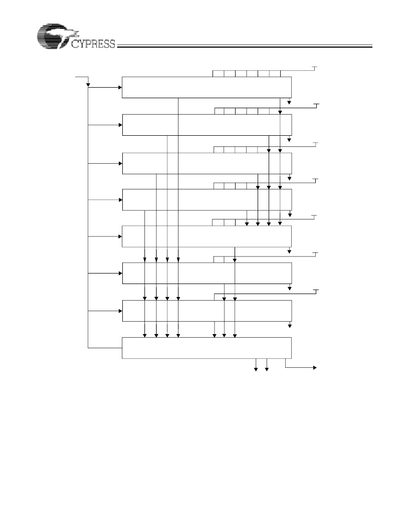
Figure 14-3. FULL Generation in a Cascaded Table
相關(guān)PDF資料 |
PDF描述 |
|---|---|
| CYNSE70256 | Network Processing |
| CZET101 | Clock Driver |
| CZEU101 | Quad Peripheral Driver |
| CZEZ101 | Triple Peripheral Driver |
| CZSP103 | Voltage Reference |
相關(guān)代理商/技術(shù)參數(shù) |
參數(shù)描述 |
|---|---|
| CYNSE70128-83BGC | 制造商:Cypress Semiconductor 功能描述:NETWORK SEARCH ENGINE 388BGA - Trays |
| CYNSE70128-83BGI | 制造商:Cypress Semiconductor 功能描述:NETWORK SEARCH ENGINE 388BGA - Trays |
| CYNSE70129HV-200BGC | 制造商:Cypress Semiconductor 功能描述: |
| CYNSE70131-250BBC | 制造商:Cypress Semiconductor 功能描述: |
| CYNSE70131A-250BBC | 制造商:Cypress Semiconductor 功能描述: |
發(fā)布緊急采購(gòu),3分鐘左右您將得到回復(fù)。