- 您現(xiàn)在的位置:買賣IC網(wǎng) > PDF目錄379089 > CY7C1916BV18 (Cypress Semiconductor Corp.) 18-Mbit DDR-II SRAM 2-Word Burst Architecture(2字Burst結(jié)構(gòu),18-Mbit DDR-II SRAM) PDF資料下載
參數(shù)資料
| 型號(hào): | CY7C1916BV18 |
| 廠商: | Cypress Semiconductor Corp. |
| 英文描述: | 18-Mbit DDR-II SRAM 2-Word Burst Architecture(2字Burst結(jié)構(gòu),18-Mbit DDR-II SRAM) |
| 中文描述: | 18兆位的DDR - II SRAM的2字突發(fā)架構(gòu)(2字突發(fā)結(jié)構(gòu),18 -兆位的DDR - II SRAM的) |
| 文件頁數(shù): | 19/28頁 |
| 文件大小: | 469K |
| 代理商: | CY7C1916BV18 |
第1頁第2頁第3頁第4頁第5頁第6頁第7頁第8頁第9頁第10頁第11頁第12頁第13頁第14頁第15頁第16頁第17頁第18頁當(dāng)前第19頁第20頁第21頁第22頁第23頁第24頁第25頁第26頁第27頁第28頁
CY7C1316BV18
CY7C1916BV18
CY7C1318BV18
CY7C1320BV18
Document Number: 38-05621 Rev. *C
Page 19 of 28
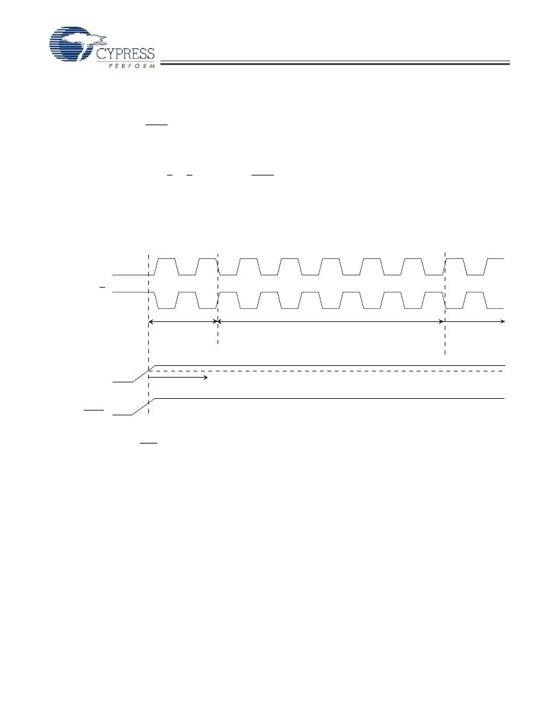
Power-Up Sequence in DDR-II SRAM
[15, 16]
DDR-II SRAMs must be powered up and initialized in a
predefined manner to prevent undefined operations.
Power-Up Sequence
Apply power and drive DOFF LOW (All other inputs can be
HIGH or LOW)
— Apply V
DD
before V
DDQ
— Apply V
DDQ
before V
REF
or at the same time as V
REF
After the power and clock (K, K, C, C) are stable take DOFF
HIGH
The additional 1024 cycles of clocks are required for the
DLL to lock
DLL Constraints
DLL uses either K or C clock as its synchronizing input.The
input should have low phase jitter, which is specified as
t
KC Var
The DLL will function at frequencies down to 80 MHz
If the input clock is unstable and the DLL is enabled, then
the DLL may lock to an incorrect frequency, causing
unstable SRAM behavior
Notes:
15.It is recommended that the DOFF pin be pulled HIGH via a pull up resistor of 1 Kohm.
16.During Power-Up, when the DOFF is tied HIGH, the DLL gets locked after 1024 cycles of stable clock.
Power-up Waveforms
> 1024 Stable clock
Start Normal
Operation
DOFF
Stabl
e
(< +/- 0.1V DC per 50ns )
Fix High (or tied to VDDQ)
K
K
DDQ
V
DD
V
/
DDQ
DD
V
V
/
Clock Start
(
Clock Starts after DD
)
V
/
~
~
~
~
Unstable Clock
相關(guān)PDF資料 |
PDF描述 |
|---|---|
| CY7C1320BV18 | 18-Mbit DDR-II SRAM 2-Word Burst Architecture(2字Burst結(jié)構(gòu),18-Mbit DDR-II SRAM) |
| CY7C1316BV18 | 18-Mbit DDR-II SRAM 2-Word Burst Architecture(2字Burst結(jié)構(gòu),18-Mbit DDR-II SRAM) |
| CY7C1318BV18 | 18-Mbit DDR-II SRAM 2-Word Burst Architecture(2字Burst結(jié)構(gòu),18-Mbit DDR-II SRAM) |
| CY7C192 | 64K x 4 Static RAM with Separate I/O(帶獨(dú)立的輸入/輸出口的64K x 4靜態(tài) RAM) |
| CY7C194B | 256 Kb (64K x 4) Static RAM |
相關(guān)代理商/技術(shù)參數(shù) |
參數(shù)描述 |
|---|---|
| CY7C192-15VCT | 制造商:Cypress Semiconductor 功能描述: |
| CY7C192-15VXC | 功能描述:靜態(tài)隨機(jī)存取存儲(chǔ)器 64Kx4 SEP IO 靜態(tài)隨機(jī)存取存儲(chǔ)器 RoHS:否 制造商:Cypress Semiconductor 存儲(chǔ)容量:16 Mbit 組織:1 M x 16 訪問時(shí)間:55 ns 電源電壓-最大:3.6 V 電源電壓-最小:2.2 V 最大工作電流:22 uA 最大工作溫度:+ 85 C 最小工作溫度:- 40 C 安裝風(fēng)格:SMD/SMT 封裝 / 箱體:TSOP-48 封裝:Tray |
| CY7C192-15VXCT | 功能描述:靜態(tài)隨機(jī)存取存儲(chǔ)器 64Kx4 SEP IO 靜態(tài)隨機(jī)存取存儲(chǔ)器 RoHS:否 制造商:Cypress Semiconductor 存儲(chǔ)容量:16 Mbit 組織:1 M x 16 訪問時(shí)間:55 ns 電源電壓-最大:3.6 V 電源電壓-最小:2.2 V 最大工作電流:22 uA 最大工作溫度:+ 85 C 最小工作溫度:- 40 C 安裝風(fēng)格:SMD/SMT 封裝 / 箱體:TSOP-48 封裝:Tray |
| CY7C192-25DMB | 制造商:Cypress Semiconductor 功能描述:SRAM Chip Async Dual 5V 256K-Bit 64K x 4-Bit 25ns 28-Pin CDIP |
| CY7C192-35VC | 制造商:Cypress Semiconductor 功能描述: |
發(fā)布緊急采購,3分鐘左右您將得到回復(fù)。