- 您現(xiàn)在的位置:買賣IC網(wǎng) > PDF目錄379059 > CY7C1304V25 (Cypress Semiconductor Corp.) 9-Mb Pipelined SRAM with QDR Architecture(帶QDR結(jié)構(gòu)的9-M位流水線式 SRAM) PDF資料下載
參數(shù)資料
| 型號(hào): | CY7C1304V25 |
| 廠商: | Cypress Semiconductor Corp. |
| 英文描述: | 9-Mb Pipelined SRAM with QDR Architecture(帶QDR結(jié)構(gòu)的9-M位流水線式 SRAM) |
| 中文描述: | 9 - MB的流水線架構(gòu)的SRAM與國防評(píng)估報(bào)告(帶國防評(píng)估報(bào)告結(jié)構(gòu)的9米位流水線式的SRAM) |
| 文件頁數(shù): | 1/23頁 |
| 文件大?。?/td> | 216K |
| 代理商: | CY7C1304V25 |
Advanced Information
9-Mb Pipelined SRAM with QDR Architecture
Functional Description
CY7C1304V25
Cypress Semiconductor Corporation
3901 North First Street
San Jose
CA 95134
February 15, 2000
408-943-2600
5
Features
Separate Independent Read and Write Data Ports
—Supports concurrent transactions
167 MHz Clock for High Bandwidth
—2.5 ns Clock-to-Valid access time
4-Word Burst for reducing address bus frequency
Double Data Rate (DDR) interfaces on both Read &
Write Ports (data transferred at 333 MHz) @167 MHz
Two input clocks (K and K) for precise DDR timing
—SRAM uses rising edges only
Two output clocks (C and C) accounts for clock skew
and flight time mis-matches
Single multiplexed address input bus latches address
inputs for both READ and WRITE ports
Separate Port Selects for depth expansion
Synchronous internally self-timed writes
2.5V core power supply with HSTL Inputs and Outputs
13x15 mm 1.0 mm pitch fBGA package, 165 ball (11x15
matrix)
Variable drive HSTL output buffers
Expanded HSTL output voltage (1.4V-1.9V)
JTAG Interface
The CY7C1304V25 is a 2.5V Synchronous Pipelined SRAM
equipped with QDR architecture. QDR architecture consists of
two separate ports to access the memory array. The Read port
has dedicated Data Outputs to support Read operations and
the Write Port has dedicated Data Inputs to support Write op-
erations. QDR architecture has separate data inputs and data
outputs to completely eliminate the need to “turn-around” the
data bus required with common I/O devices. Access to each
port is accomplished through a common address bus. Ad-
dresses for Read and Write addresses are latched on alter-
nate rising edges of the input (K) clock. Accesses to the
CY7C1304V25 Read and Write ports are completely indepen-
dent of one another. In order to maximize data throughput,
both Read and Write ports are equipped with Double Data
Rate (DDR) interfaces. Each address location is associated
with 4 18-bit words that burst sequentially into or out of the
device. Since data can be transferred into and out of the device
on every rising edge of both input clocks (K/K and C/C) mem-
ory bandwidth is maximized while simplifying system design
by eliminating bus “turn-arounds”.
Depth expansion is accomplished with Port Selects for each
port. Port selects allow each port to operate independently.
All synchronous inputs pass through input registers controlled
by the K or K input clocks. All data outputs pass through output
registers controlled by the C or C input clocks. Writes are con-
ducted with on-chip synchronous self-timed write circuitry.
Selection Guide
7C1304V25-167
7C1304V25-133
7C1304V25-100
Maximum Operating Frequency (MHz)
167
133
100
Maximum Operating Current (mA)
450
350
230
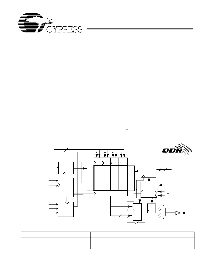
Logic Block Diagram
1
CLK
Gen.
A
(16:0)
K
K
Control
Logic
Address
Register
D
[17:0]
R
Read Data Reg.
RPS
WPS
BWS
[0:1]
Q
[17:0]
Control
Logic
Address
Register
Reg.
Reg.
Reg.
36
17
18
72
18
Vref
W
Write
Reg
36
A
(16:0)
17
C
C
1
1
1
Write
Reg
Write
Reg
Write
Reg
18
相關(guān)PDF資料 |
PDF描述 |
|---|---|
| CY7C1305BV25-100BZC | 18-Mbit Burst of 4 Pipelined SRAM with QDR Architecture |
| CY7C1307BV25 | 18-Mbit Burst of 4 Pipelined SRAM with QDR Architecture |
| CY7C1307BV25-100BZC | 18-Mbit Burst of 4 Pipelined SRAM with QDR Architecture |
| CY7C1307BV25-133BZC | 18-Mbit Burst of 4 Pipelined SRAM with QDR Architecture |
| CY7C1307BV25-167BZC | 18-Mbit Burst of 4 Pipelined SRAM with QDR Architecture |
相關(guān)代理商/技術(shù)參數(shù) |
參數(shù)描述 |
|---|---|
| CY7C1304V25-200BZC | 制造商:Cypress Semiconductor 功能描述:9MB PIPELINE QDR SRAM 2.5V CORE, FBGA - Trays |
| CY7C1305 WAF | 制造商:Cypress Semiconductor 功能描述: |
| CY7C13055DC | 制造商:CYPRESS 功能描述:* |
| CY7C130-55PC | 功能描述:靜態(tài)隨機(jī)存取存儲(chǔ)器 1K x 8 Dual-Port 靜態(tài)隨機(jī)存取存儲(chǔ)器 RoHS:否 制造商:Cypress Semiconductor 存儲(chǔ)容量:16 Mbit 組織:1 M x 16 訪問時(shí)間:55 ns 電源電壓-最大:3.6 V 電源電壓-最小:2.2 V 最大工作電流:22 uA 最大工作溫度:+ 85 C 最小工作溫度:- 40 C 安裝風(fēng)格:SMD/SMT 封裝 / 箱體:TSOP-48 封裝:Tray |
| CY7C1305BV25-167BZC | 功能描述:靜態(tài)隨機(jī)存取存儲(chǔ)器 1Mx18 2.5V QDR 靜態(tài)隨機(jī)存取存儲(chǔ)器 COM RoHS:否 制造商:Cypress Semiconductor 存儲(chǔ)容量:16 Mbit 組織:1 M x 16 訪問時(shí)間:55 ns 電源電壓-最大:3.6 V 電源電壓-最小:2.2 V 最大工作電流:22 uA 最大工作溫度:+ 85 C 最小工作溫度:- 40 C 安裝風(fēng)格:SMD/SMT 封裝 / 箱體:TSOP-48 封裝:Tray |
發(fā)布緊急采購,3分鐘左右您將得到回復(fù)。