- 您現(xiàn)在的位置:買賣IC網(wǎng) > PDF目錄378482 > CY28341-2 (Cypress Semiconductor Corp.) Universal Clock Chip for VIA P4M/KT/KM400 DDR Systems PDF資料下載
參數(shù)資料
| 型號(hào): | CY28341-2 |
| 廠商: | Cypress Semiconductor Corp. |
| 英文描述: | Universal Clock Chip for VIA P4M/KT/KM400 DDR Systems |
| 中文描述: | 通用時(shí)鐘芯片的威盛P4M/KT/KM400的DDR系統(tǒng) |
| 文件頁數(shù): | 15/19頁 |
| 文件大小: | 174K |
| 代理商: | CY28341-2 |
CY28341-2
Document #: 38-07471 Rev. *B
Page 15 of 19
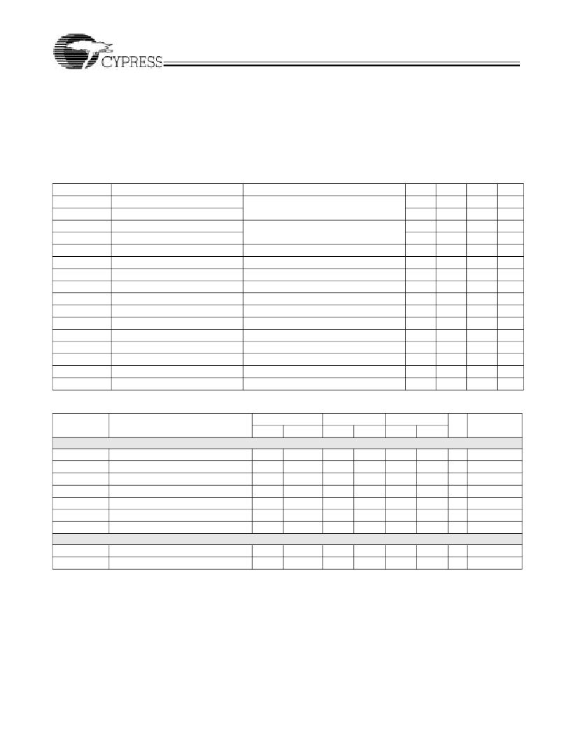
Maximum Ratings
[5]
Input Voltage Relative to V
SS
:.............................. V
SS
– 0.3V
Input Voltage Relative to V
DDQ
or AV
DD
: .............V
DD
+ 0.3V
Storage Temperature: ................................–65
°
C to + 150
°
C
Operating Temperature:....................................0
°
C to +70
°
C
Maximum ESD.............................................................2000V
Maximum Power Supply: ................................................5.5V
DC Parameters
(
VDD=VDDPCI=VDDAGP=VDDR=VDD48M=VDDC= 3.3v±5%, VDDI = VDD=2.5±5%, TA=0°C TO +70°C)
This device contains circuitry to protect the inputs against
damage due to high static voltages or electric field. However,
precautions should be take to avoid application of any voltage
higher than the maximum rated voltages to this circuit. For
proper operation, V
IN
and V
OUT
should be constrained to the
range:
V
SS
< (V
IN
or V
OUT
) < V
DD
.
Unused inputs must always be tied to an appropriate logic
voltage level (either V
SS
or V
DD
).
Parameter
V
IL1
V
IH1
V
IL2
V
IH2
V
OL
I
OL
I
OZ
I
DD3.3V
I
DD2.5V
I
PD
I
I
PDWN
C
IN
C
OUT
L
PIN
C
XTAL
Description
Conditions
Min.
Typ.
Max.
0.8
Unit
Vdc
Vdc
Vdc
Vdc
V
mA
μ
A
mA
mA
μ
A
μ
A
μ
A
pF
pF
pF
pF
Input Low Voltage
Input High Voltage
Input Low Voltage
Input High Voltage
Output Low Voltage for SRESET# I
OL
Pull-down current for SRESET#
Three-state leakage Current
Dynamic Supply Current
Dynamic Supply Current
Power-down Supply current
Internal Pull-up Device Current
Internal Pull-down Device Current Input @ V
DD
Input pin capacitance
Output pin capacitance
Pin Inductance
Crystal pin capacitance
Applicable to PD#, F S(0:4)
2.0
Applicable to SDATA and SCLK
1.0
2.2
0.4
24
V
OL
= 0.4V
35
10
190
195
600
–25
10
5
6
7
45
CPU frequency set at 133.3 MHz,
Note 6
CPU frequency set at 133.3 MHz,
Note 6
PD# = 0
Input @ V
SS
150
175
95
Measured from the Xin or Xout to V
SS
27
36
AC Parameters
Parameter
XTAL
T
DC
T
PERIOD
V
HIGH
V
LOW
T
R
/T
F
T
CCJ
T
XS
P4 Mode CPU at 0.7V
T
DC
T
PERIOD
Notes:
5.
Multiple Supplies:
The voltage on any input or I/O pin cannot exceed the power pin during power-up. Power supply sequencing is NOT required.
6.
All outputs loaded as per maximum capacitive load table.
7.
This parameter is measured as an average over a 1-us duration, with a crystal center frequency of 14.31818 MHz.
8.
All outputs loaded as per loading specified in the
Table 11
.
9.
Probes are placed on the pins, and measurements are acquired at 1.5V for 3.3V signals and at 1.25V for 2.5V, and 50% point for differential signals.
10. Probes are placed on the pins, and measurements are acquired at 0.4V.
11.
When Xin is driven from and external clock source (3.3V parameters apply).
12. When crystal meets minimum 40-ohm device series resistance specification.
13. Measured between 0.2V
and.7V
.
14. This is required for the duty cycle on the REF clock out to be as specified. The device will operate reliably with input duty cycles up to 30/70 but the REF clock
duty cycle will not be within data sheet specifications.
15. Measured at VX, or where subtraction of CLK-CLK# crosses 0V.
16. See
Figure 10
for 0.7V loading specification.
Description
100 MHz
Min.
133 MHz
Min.
200 MHz
Min.
Unit
Notes
Max.
Max
Max.
Xin Duty Cycle
Xin Period
Xin High Voltage
Xin Low Voltage
Xin Rise and Fall Times
Xin Cycle to Cycle Jitter
Crystal Start-up Time
45
55
45
55
71.0
V
DD
.3V
DD
10
500
30
45
55
71.0
V
DD
.3V
DD
10
500
30
% 7,14
ns 7,14
V
12
V
15
ns 13
ps 8,11
ms 10,12
69.84
.7V
DD
0
71.00
V
DD
.3V
DD
10.0
500
30
69.84
.7V
DD
0
69.84
.7V
DD
0
CPUT/C Duty Cycle
CPUT/C Period
45
9.85
55
10.2
45
7.35
55
7.65
45
4.85
55
5.1
% 7,8,9,15, 16
ns 7,8,9,15, 16
相關(guān)PDF資料 |
PDF描述 |
|---|---|
| CY29962 | 2.5V/3.3V, 150-MHz Multi-Output Zero Delay Buffer |
| CY30 | Sensor interface for an inductive engine wheel speed single rotation sensor |
| CY37128V | 5V, 3.3V, ISR⑩ High-Performance CPLDs |
| CY37256V | 5V, 3.3V, ISR⑩ High-Performance CPLDs |
| CY54FCT138CTDMB | 1-of-8 Decoder |
相關(guān)代理商/技術(shù)參數(shù) |
參數(shù)描述 |
|---|---|
| CY28341-2_05 | 制造商:CYPRESS 制造商全稱:Cypress Semiconductor 功能描述:Universal Clock Chip for VIA⑩P4M/KT/KM400 DDR Systems |
| CY28341-3 | 制造商:CYPRESS 制造商全稱:Cypress Semiconductor 功能描述:Universal Clock Chip for VIA⑩P4M/KT/KM400A DDR Systems |
| CY28341OC | 制造商:Rochester Electronics LLC 功能描述:FTG FOR VIA P4 CHIPSET - Bulk |
| CY28341OC-2 | 制造商:Rochester Electronics LLC 功能描述:- Bulk |
| CY28341OC-2T | 制造商:CYPRESS 制造商全稱:Cypress Semiconductor 功能描述:Universal Clock Chip for VIA⑩P4M/KT/KM400 DDR Systems |
發(fā)布緊急采購,3分鐘左右您將得到回復(fù)。