- 您現(xiàn)在的位置:買賣IC網(wǎng) > PDF目錄378482 > CY28341-2 (Cypress Semiconductor Corp.) Universal Clock Chip for VIA P4M/KT/KM400 DDR Systems PDF資料下載
參數(shù)資料
| 型號: | CY28341-2 |
| 廠商: | Cypress Semiconductor Corp. |
| 英文描述: | Universal Clock Chip for VIA P4M/KT/KM400 DDR Systems |
| 中文描述: | 通用時鐘芯片的威盛P4M/KT/KM400的DDR系統(tǒng) |
| 文件頁數(shù): | 10/19頁 |
| 文件大小: | 174K |
| 代理商: | CY28341-2 |
CY28341-2
Document #: 38-07471 Rev. *B
Page 10 of 19
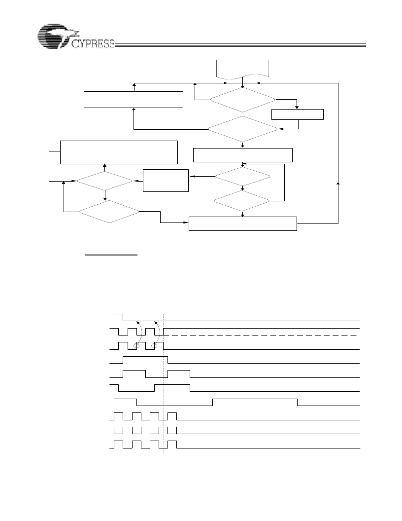
P4 Processor SELP4_K7# = 1
Power-down Assertion (P4 Mode)
:
When PD# is sampled low by two consecutive rising edges of
CPU# clock then all clock outputs except CPU clocks must be
held low on their next high to low transition. CPU clocks must
be held with the CPU clock pin driven high with a value of 2 x
Iref, and CPU# undriven. Note that
Figure 1
shows CPU =
133 MHz. This diagram and description are applicable for all
valid CPU frequencies 66, 100, 133, 200 MHz. Due to the state
of internal logic, stopping and holding the REF clock outputs
in the LOW state may require more than one clock cycle to
complete.
S y s t e m r u n n in g w it h
o r ig in a lly s e le c t e d
f r e q u e n c y v ia
h a r d w a r e s t r a p p in g .
R e c e iv e F r e q u e n c y
C h a n g e R e q u e s t v ia
S M B u s B y t e 4 o r V ia D ia l-
a - f r e q u e n c y
S t a r t in t e r n a l w a t c h d o g t im e r .
W a t c h D o g t im e o u t
T u r n o f f w a t c h d o g t im e r .
K e e p n e w f r e q u e n c y s e t t in g . S e t W D a la r m
b it ( b y t e 1 2 , b it 4 ) t o ''0 '
1 ) S e n d a n o t h e r 3 m S lo w p u ls e o n S R E S E T
2 ) R e la t c h o r ig in a l h a r d w a r e s t r a p p in g s e le c t io n
f o r r e t u r n t o o r ig in a l f r e q u e n c y s e t t in g s .
3 ) S e t W D A la r m b it ( b y t e 1 2 , B it 4 ) t o " 1 "
4 ) S t a r t W D t im e r
F r e q u e n c y w ill c h a n g e b u t S y s t e m S e lf
R e c o v e r y n o t a p p lic a b le ( n o t im e s t a m p
s e le c t e d a n d b y t e 1 2 , b it ( 3 : 0 ) is s t ill =
" 0 0 0 0 "
N o
N o
Y e s
N o
N o
Y e s
S M B u s b y t e 1 2 t im e
o u t s t a m p d is a b le d
I s S M B u s B y t e 9 , t im e o u t
s t a m p e n a b le d - ( b y t e 1 2 , b it
( 3 : 0 ) 0 0 0 0 )
C h a n g e t o a n e w
f r e q u e n c y
Y e s
1 ) S e n d S R E S E T
p u ls e
2 ) S e t W D b it
( b y t e 1 2 , b it 4 ) t o '1 '
3 ) S t a r t W D t im e r
Y e s
W a t c h D o g t im e o u t
N o
Y e s
S M B u s b y t e 9 t im e o u t
s t a m p d is a b le d , B y t e
1 2 , b it ( 3 : 0 ) = ( 0 0 0 0 )
Y e s
N o
Figure 1. Watchdog Recovery Clock
PCI 33M Hz
PW RD W N #
CPUT 133M Hz
CPUT# 133M Hz
REF 14.318M Hz
USB 48M Hz
SD RAM 133M Hz
D DRT 133M Hz
DDR C 133M Hz
AG P 66M Hz
Figure 2. Power-down Assertion Timing Waveform (in P4 mode)
相關(guān)PDF資料 |
PDF描述 |
|---|---|
| CY29962 | 2.5V/3.3V, 150-MHz Multi-Output Zero Delay Buffer |
| CY30 | Sensor interface for an inductive engine wheel speed single rotation sensor |
| CY37128V | 5V, 3.3V, ISR⑩ High-Performance CPLDs |
| CY37256V | 5V, 3.3V, ISR⑩ High-Performance CPLDs |
| CY54FCT138CTDMB | 1-of-8 Decoder |
相關(guān)代理商/技術(shù)參數(shù) |
參數(shù)描述 |
|---|---|
| CY28341-2_05 | 制造商:CYPRESS 制造商全稱:Cypress Semiconductor 功能描述:Universal Clock Chip for VIA⑩P4M/KT/KM400 DDR Systems |
| CY28341-3 | 制造商:CYPRESS 制造商全稱:Cypress Semiconductor 功能描述:Universal Clock Chip for VIA⑩P4M/KT/KM400A DDR Systems |
| CY28341OC | 制造商:Rochester Electronics LLC 功能描述:FTG FOR VIA P4 CHIPSET - Bulk |
| CY28341OC-2 | 制造商:Rochester Electronics LLC 功能描述:- Bulk |
| CY28341OC-2T | 制造商:CYPRESS 制造商全稱:Cypress Semiconductor 功能描述:Universal Clock Chip for VIA⑩P4M/KT/KM400 DDR Systems |
發(fā)布緊急采購,3分鐘左右您將得到回復(fù)。