- 您現(xiàn)在的位置:買賣IC網(wǎng) > PDF目錄378405 > AND8090D (ON SEMICONDUCTOR) AC Characteristics of ECL Devices PDF資料下載
參數(shù)資料
| 型號(hào): | AND8090D |
| 廠商: | ON SEMICONDUCTOR |
| 英文描述: | AC Characteristics of ECL Devices |
| 中文描述: | 交流特性的ECL裝置 |
| 文件頁(yè)數(shù): | 9/20頁(yè) |
| 文件大小: | 896K |
| 代理商: | AND8090D |
第1頁(yè)第2頁(yè)第3頁(yè)第4頁(yè)第5頁(yè)第6頁(yè)第7頁(yè)第8頁(yè)當(dāng)前第9頁(yè)第10頁(yè)第11頁(yè)第12頁(yè)第13頁(yè)第14頁(yè)第15頁(yè)第16頁(yè)第17頁(yè)第18頁(yè)第19頁(yè)第20頁(yè)
AND8090/D
http://onsemi.com
9
Differential Inputs (SingleEnded Mode)
– Either input
of a differential pair may be used individually if the unused
input of the differential pair is connected to V
BB
(the
switching reference voltage). The switching reference
voltage is provided by many differential devices. Figure 19
illustrates the use of the true input as the singleended input.
Note that the unused inverted output is terminated in the
same fashion as the true output.
Figure 19. Differential Input in SingleEnded Mode
V
IH
V
IL
50%
50%
V
OH
V
OL
D1
D1
V
BB
Q1
Q1
Use Q1 Termination
The switching reference voltage provides a switching
point that is approximately halfway between the HIGH and
LOW levels. As an example, the MC100EP116 data sheet
specifies the following switching reference voltage range
for the 5.0 V PECL mode. The MC100EP116 50% point
range previously calculated is listed below the V
BB
range.
3475 mV
VBB
3675 mV
3483 mV
50% Point
3748 mV
Note that the V
BB
range is very close to the 50% point
range. This is true because the switching reference voltage
provides a switching point for a differential input in
singleended mode that is analogous to the 50% point range
for normal singleended inputs.
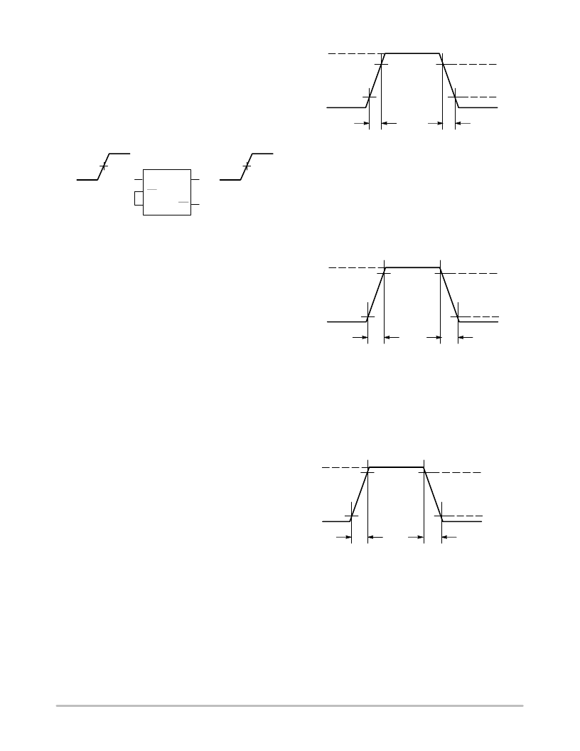
TIMING CHARACTERISTICS
Output Rise and Fall Times
ECL Output Devices
– The output rise time for ECL
devices is the time required to rise from the 20% level to the
80% level of the output rising edge. The output fall time for
ECL devices is the time required to fall from the 80% level
to the 20% level of the output falling edge. The output rise
and fall times for devices with ECL outputs is shown in
Figure 20.
Figure 20. ECL Output Rise and Fall Times
t
R
t
F
HIGH
LOW
20%
80%
NonECL Output Devices
– Refer to the translator data
sheets as different conditions are used to specify the output
rise and fall times. One type of condition specifies output
rise and fall times between the 10% and 90% output levels.
For example, the rise and fall times for the MC100ELT21
PECL to TTL translator are specified between the 10% and
90% output levels as shown in Figure 21.
Figure 21. TTL Output Rise and Fall
Time Percentages
t
R
t
F
90%
10%
HIGH
LOW
Another type of test condition specifies nonECL output
rise and fall times between fixed output voltage levels. For
example, the rise and fall times for the MC100EPT21
LVPECL to LVTTL translator are specified between fixed
output voltages of 0.8 V and 2.0 V as shown in Figure 22.
Figure 22. LVTTL Output Rise and Fall
Time Levels
t
R
t
F
HIGH
LOW
V
O
= 2.0 V
V
O
= 0.8 V
相關(guān)PDF資料 |
PDF描述 |
|---|---|
| AND8094 | Three New Tiny Switches Facilitate Video Switching |
| AND8094D | Three New Tiny Switches Facilitate Video Switching |
| AND8098 | Low-Cost 100 mA High-Voltage Buck and Buck-Boost Using NCP1052 |
| AND8099 | 5.0 V, 2.0 A Flyback Converter |
| AND8109 | LED CONSTANT CURRENT SOURCE SCHEME |
相關(guān)代理商/技術(shù)參數(shù) |
參數(shù)描述 |
|---|---|
| AND8094 | 制造商:ONSEMI 制造商全稱:ON Semiconductor 功能描述:Three New Tiny Switches Facilitate Video Switching |
| AND8094D | 制造商:ONSEMI 制造商全稱:ON Semiconductor 功能描述:Three New Tiny Switches Facilitate Video Switching |
| AND8098 | 制造商:ONSEMI 制造商全稱:ON Semiconductor 功能描述:Low-Cost 100 mA High-Voltage Buck and Buck-Boost Using NCP1052 |
| AND8099 | 制造商:ONSEMI 制造商全稱:ON Semiconductor 功能描述:5.0 V, 2.0 A Flyback Converter |
| AND8099/D | 制造商:ONSEMI 制造商全稱:ON Semiconductor 功能描述:5.0 V, 2.0 A Flyback Converter |
發(fā)布緊急采購(gòu),3分鐘左右您將得到回復(fù)。