- 您現(xiàn)在的位置:買賣IC網(wǎng) > PDF目錄366550 > AM79C930VCW (ADVANCED MICRO DEVICES INC) PCnet-Mobile Single-Chip Wireless LAN Media Access Controller PDF資料下載
參數(shù)資料
| 型號(hào): | AM79C930VCW |
| 廠商: | ADVANCED MICRO DEVICES INC |
| 元件分類: | 微控制器/微處理器 |
| 英文描述: | PCnet-Mobile Single-Chip Wireless LAN Media Access Controller |
| 中文描述: | 2 CHANNEL(S), LOCAL AREA NETWORK CONTROLLER, PQFP144 |
| 封裝: | TQFP-144 |
| 文件頁(yè)數(shù): | 38/161頁(yè) |
| 文件大小: | 691K |
| 代理商: | AM79C930VCW |
第1頁(yè)第2頁(yè)第3頁(yè)第4頁(yè)第5頁(yè)第6頁(yè)第7頁(yè)第8頁(yè)第9頁(yè)第10頁(yè)第11頁(yè)第12頁(yè)第13頁(yè)第14頁(yè)第15頁(yè)第16頁(yè)第17頁(yè)第18頁(yè)第19頁(yè)第20頁(yè)第21頁(yè)第22頁(yè)第23頁(yè)第24頁(yè)第25頁(yè)第26頁(yè)第27頁(yè)第28頁(yè)第29頁(yè)第30頁(yè)第31頁(yè)第32頁(yè)第33頁(yè)第34頁(yè)第35頁(yè)第36頁(yè)第37頁(yè)當(dāng)前第38頁(yè)第39頁(yè)第40頁(yè)第41頁(yè)第42頁(yè)第43頁(yè)第44頁(yè)第45頁(yè)第46頁(yè)第47頁(yè)第48頁(yè)第49頁(yè)第50頁(yè)第51頁(yè)第52頁(yè)第53頁(yè)第54頁(yè)第55頁(yè)第56頁(yè)第57頁(yè)第58頁(yè)第59頁(yè)第60頁(yè)第61頁(yè)第62頁(yè)第63頁(yè)第64頁(yè)第65頁(yè)第66頁(yè)第67頁(yè)第68頁(yè)第69頁(yè)第70頁(yè)第71頁(yè)第72頁(yè)第73頁(yè)第74頁(yè)第75頁(yè)第76頁(yè)第77頁(yè)第78頁(yè)第79頁(yè)第80頁(yè)第81頁(yè)第82頁(yè)第83頁(yè)第84頁(yè)第85頁(yè)第86頁(yè)第87頁(yè)第88頁(yè)第89頁(yè)第90頁(yè)第91頁(yè)第92頁(yè)第93頁(yè)第94頁(yè)第95頁(yè)第96頁(yè)第97頁(yè)第98頁(yè)第99頁(yè)第100頁(yè)第101頁(yè)第102頁(yè)第103頁(yè)第104頁(yè)第105頁(yè)第106頁(yè)第107頁(yè)第108頁(yè)第109頁(yè)第110頁(yè)第111頁(yè)第112頁(yè)第113頁(yè)第114頁(yè)第115頁(yè)第116頁(yè)第117頁(yè)第118頁(yè)第119頁(yè)第120頁(yè)第121頁(yè)第122頁(yè)第123頁(yè)第124頁(yè)第125頁(yè)第126頁(yè)第127頁(yè)第128頁(yè)第129頁(yè)第130頁(yè)第131頁(yè)第132頁(yè)第133頁(yè)第134頁(yè)第135頁(yè)第136頁(yè)第137頁(yè)第138頁(yè)第139頁(yè)第140頁(yè)第141頁(yè)第142頁(yè)第143頁(yè)第144頁(yè)第145頁(yè)第146頁(yè)第147頁(yè)第148頁(yè)第149頁(yè)第150頁(yè)第151頁(yè)第152頁(yè)第153頁(yè)第154頁(yè)第155頁(yè)第156頁(yè)第157頁(yè)第158頁(yè)第159頁(yè)第160頁(yè)第161頁(yè)
AMD
P R E L I M I N A R Y
38
Am79C930
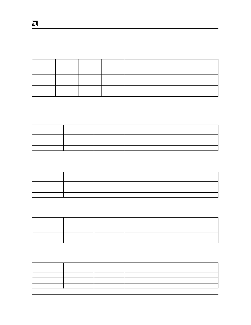
Pin 101: SDCLK
The SDCLK pin may be configured for input or output
operation. The output drive may be programmed for reg-
ister-driven or auto-pulse generation. The auto-pulse
may be programmed for either active low or active high
operation. SDCLK pin configuration is accomplished ac-
cording to the following table:
Note that a read of the SDC bit (TIR2[2]) will always
give the current SDCLK pin value, regardless of pin
configuration setting.
SDCLKEN
TCR13[4]
0
1
1
1
1
SDCP
TIR2[3]
X
0
1
0
1
SDC
TIR2[2]
X
0
0
1
1
SDCLK Pin
Direction
I
O
O
O
O
SDCLK Pin
Value
NA
LOW
HIGH active pulse
HIGH
LOW active pulse
reset default condition
(when write to TIR2 occurs)
(when write to TIR2 occurs)
Pin 102: SDDATA
The SDDATA pin may be configured for input or output
operation. SDDATA pin configuration is accomplished
according to the following table:
Note that a read of the SDD bit (TIR2[0]) will always
give the current SDDATA pin value, regardless of pin
configuration setting.
SDDT
TIR2[1]
0
0
1
SDD
TIR2[0]
0
1
X
SDDATA Pin
Direction
O
O
I
SDDATA Pin
Value
LOW
HIGH
NA
reset default condition
Pin 103:
SDSEL3
The
SDSEL
[
3
] pin may be configured for input or output
operation according to the following table:
Note that a read of the SDS[3] bit (TIR2[6]) will always
give the current
SDSEL
[
3
] pin value without inversion,
regardless of pin configuration setting.
SDSEL3
EN
TCR13[3]
0
1
1
SDS[
3
]
TIR2[6]
X
0
1
SDSEL
[
3
]
Pin Direction
I
O
O
SDSEL
[
3
]
Pin Value
NA
HIGH
LOW
reset default condition
Pin 105:
SDSEL2
The
SDSEL
[
2
] pin may be configured for input or output
operation according to the following table:
Note that a read of the SDS[2] bit (TIR2[5]) will always
give the current
SDSEL
[
2
] pin value without inversion,
regardless of pin configuration setting.
SDSEL2
EN
TCR13[2]
0
1
1
SDS[
2
]
TIR2[5]
X
0
1
SDSEL
[
2
]
Pin Direction
I
O
O
SDSEL
[
2
]
Pin Value
NA
HIGH
LOW
reset default condition
Pin 107:
SDSEL1
The
SDSEL
[
1
] pin may be configured for input or output
operation according to the following table:
Note that a read of the SDS[1] bit (TIR2[4]) will always
give the current
SDSEL
[
1
] pin value without inversion,
regardless of pin configuration setting.
SDSEL1
EN
TCR13[1]
0
1
1
SDS[1]
TIR2[4]
X
0
1
SDSEL
[1]
Pin Direction
I
O
O
SDSEL
[1]
Pin Value
NA
HIGH
LOW
reset default condition
相關(guān)PDF資料 |
PDF描述 |
|---|---|
| AM79C940VCW | Media Access Controller for Ethernet (MACE) |
| AM79C940 | Media Access Controller for Ethernet (MACE) |
| AM79C940JCW | Media Access Controller for Ethernet (MACE) |
| AM79C940KCW | Media Access Controller for Ethernet (MACE) |
| AM79C960 | PCnetTM-ISA Single-Chip Ethernet Controller |
相關(guān)代理商/技術(shù)參數(shù) |
參數(shù)描述 |
|---|---|
| AM79C940 | 制造商:AMD 制造商全稱:Advanced Micro Devices 功能描述:Media Access Controller for Ethernet (MACE) |
| AM79C940_00 | 制造商:AMD 制造商全稱:Advanced Micro Devices 功能描述:Media Access Controller for Ethernet (MACE⑩) |
| AM79C940-16/25 | 制造商:未知廠家 制造商全稱:未知廠家 功能描述: |
| AM79C940-16JC | 制造商:未知廠家 制造商全稱:未知廠家 功能描述:LAN Node Controller |
| AM79C940-25JC | 制造商:未知廠家 制造商全稱:未知廠家 功能描述:LAN Node Controller |
發(fā)布緊急采購(gòu),3分鐘左右您將得到回復(fù)。