- 您現(xiàn)在的位置:買(mǎi)賣(mài)IC網(wǎng) > PDF目錄373857 > AD14160BB-4 (ANALOG DEVICES INC) Quad-SHARC DSP Multiprocessor Family PDF資料下載
參數(shù)資料
| 型號(hào): | AD14160BB-4 |
| 廠商: | ANALOG DEVICES INC |
| 元件分類: | 數(shù)字信號(hào)處理 |
| 英文描述: | Quad-SHARC DSP Multiprocessor Family |
| 中文描述: | 48-BIT, 40 MHz, OTHER DSP, CBGA452 |
| 封裝: | CERAMIC, BGA-452 |
| 文件頁(yè)數(shù): | 33/52頁(yè) |
| 文件大小: | 1193K |
| 代理商: | AD14160BB-4 |
第1頁(yè)第2頁(yè)第3頁(yè)第4頁(yè)第5頁(yè)第6頁(yè)第7頁(yè)第8頁(yè)第9頁(yè)第10頁(yè)第11頁(yè)第12頁(yè)第13頁(yè)第14頁(yè)第15頁(yè)第16頁(yè)第17頁(yè)第18頁(yè)第19頁(yè)第20頁(yè)第21頁(yè)第22頁(yè)第23頁(yè)第24頁(yè)第25頁(yè)第26頁(yè)第27頁(yè)第28頁(yè)第29頁(yè)第30頁(yè)第31頁(yè)第32頁(yè)當(dāng)前第33頁(yè)第34頁(yè)第35頁(yè)第36頁(yè)第37頁(yè)第38頁(yè)第39頁(yè)第40頁(yè)第41頁(yè)第42頁(yè)第43頁(yè)第44頁(yè)第45頁(yè)第46頁(yè)第47頁(yè)第48頁(yè)第49頁(yè)第50頁(yè)第51頁(yè)第52頁(yè)
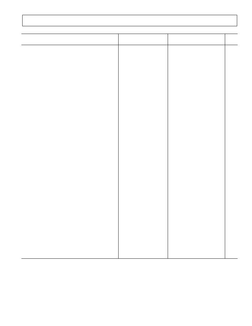
AD14160/AD14160L
–33–
REV. A
Serial Ports
40 MHz–5 V
40 MHz–3.3 V
Min
Parameter
Min
Max
Max
Units
External Clock
Timing Requirements:
t
SFSE
t
HFSE
t
SDRE
t
HDRE
t
SCLKW
t
SCLK
TFS/RFS Setup Before TCLK/RCLK
1
TFS/RFS Hold After TCLK/RCLK
1, 2
Receive Data Setup Before RCLK
1
Receive Data Hold After RCLK
1
TCLK/RCLK Width
TCLK/RCLK Period
3.5
4
1.5
4
9.5
t
CK
3.5
4
1.5
4
9
t
CK
ns
ns
ns
ns
ns
ns
Internal Clock
Timing Requirements:
t
SFSI
t
HFSI
t
SDRI
t
HDRI
TFS Setup Before TCLK
1
; RFS Setup Before RCLK
1
8
TFS/RFS Hold After TCLK/RCLK
1, 2
Receive Data Setup Before RCLK
1
Receive Data Hold After RCLK
1
8
1
3
3
ns
ns
ns
ns
1
3
3
External or Internal Clock
Switching Characteristics:
t
DFSE
RFS Delay After RCLK (Internally Generated RFS)
3
t
HFSE
RFS Hold After RCLK (Internally Generated RFS)
3
13.5
13.5
ns
ns
3
3
External Clock
Switching Characteristics:
t
DFSE
TFS Delay After TCLK (Internally Generated TFS)
3
t
HFSE
TFS Hold After TCLK (Internally Generated TFS)
3
t
DDTE
Transmit Data Delay After TCLK
3
t
HDTE
Transmit Data Hold After TCLK
3
13.5
13.5
ns
ns
ns
ns
3
3
16.5
16.5
5
5
Internal Clock
Switching Characteristics:
t
DFSI
TFS Delay After TCLK (Internally Generated TFS)
3
t
HFSI
TFS Hold After TCLK (Internally Generated TFS)
3
t
DDTI
Transmit Data Delay After TCLK
3
t
HDTI
Transmit Data Hold After TCLK
3
t
SCLKIW
TCLK/RCLK Width
4.5
4.5
ns
ns
ns
ns
ns
–1.5
–1.5
7.5
7.5
0
(SCLK/2) – 2
0
(SCLK/2) – 2.5
(SCLK/2) + 2
(SCLK/2) + 2.5
Enable and Three-State
Switching Characteristics:
t
DDTEN
Data Enable from External TCLK
3
t
DDTTE
Data Disable from External TCLK
3
t
DDTIN
Data Enable from Internal TCLK
3
t
DDTTI
Data Disable from Internal TCLK
3
t
DCLK
TCLK/RCLK Delay from CLKIN
t
DPTR
SPORT Disable After CLKIN
3.5
4
ns
ns
ns
ns
ns
ns
11
11
0
0
3
22.5 + 3DT/8
17.5
3
22.5 + 3DT/8
17.5
External Late Frame Sync
Switching Characteristics:
t
DDTLFSE
Data Delay from Late External TFS or
External RFS with MCE = 1, MFD = 0
4
t
DDTENFS
Data Enable from Late FS or MCE = 1, MFD = 0
4
12.5
13.3
ns
3
3.5
ns
To determine whether communication is possible between two devices at clock speed
n,
the following specifications must be confirmed: 1) frame sync delay and frame
sync setup and hold, 2) data delay and data setup and hold, and 3) SCLK width.
NOTES
1
Referenced to sample edge.
2
RFS hold after RCK when MCE = 1, MFD = 0 is 0 ns minimum from drive edge. TFS hold after TCK for late external TFS is 0 ns minimum from drive edge.
3
Referenced to drive edge.
4
MCE = 1, TFS enable and TFS valid follow t
DDTLFSE
and t
DDTENFS
.
相關(guān)PDF資料 |
PDF描述 |
|---|---|
| AD14160L | Quad-SHARC DSP Multiprocessor Family |
| AD14160LBB-4 | ECONOLINE: RD & RC - Dual Output from a Single Input Rail- 1kVDC & 2kVDC Isolation- Power Sharing on Output- Custom Solutions Available- UL94V-0 Package Material- Efficiency to 86% |
| AD14160LKB-4 | Quad-SHARC DSP Multiprocessor Family |
| AD1555-AD1556 | 24-Bit ADC WITH LOW NOISE PGA |
| AD1555AP | 24-Bit ADC WITH LOW NOISE PGA |
相關(guān)代理商/技術(shù)參數(shù) |
參數(shù)描述 |
|---|---|
| AD14160KB-4 | 制造商:Rochester Electronics LLC 功能描述:- Bulk |
| AD14160L | 制造商:AD 制造商全稱:Analog Devices 功能描述:Quad-SHARC DSP Multiprocessor Family |
| AD14160LBB-4 | 制造商:AD 制造商全稱:Analog Devices 功能描述:Quad-SHARC DSP Multiprocessor Family |
| AD14160LKB-4 | 制造商:Rochester Electronics LLC 功能描述:- Bulk |
| AD142 | 制造商:未知廠家 制造商全稱:未知廠家 功能描述:TRANSISTOR | BJT | PNP | 80V V(BR)CEO | 10A I(C) | TO-3 |
發(fā)布緊急采購(gòu),3分鐘左右您將得到回復(fù)。