- 您現(xiàn)在的位置:買賣IC網(wǎng) > PDF目錄294088 > 70824L35PFI (INTEGRATED DEVICE TECHNOLOGY INC) 4K X 16 STANDARD SRAM, 35 ns, PQFP80 PDF資料下載
參數(shù)資料
| 型號: | 70824L35PFI |
| 廠商: | INTEGRATED DEVICE TECHNOLOGY INC |
| 元件分類: | SRAM |
| 英文描述: | 4K X 16 STANDARD SRAM, 35 ns, PQFP80 |
| 封裝: | TQFP-80 |
| 文件頁數(shù): | 17/21頁 |
| 文件大?。?/td> | 191K |
| 代理商: | 70824L35PFI |

6.42
IDT70824S/L
High-Speed 4K x 16 Sequential Access Random Access Memory
Military and Commercial Temperature Ranges
5
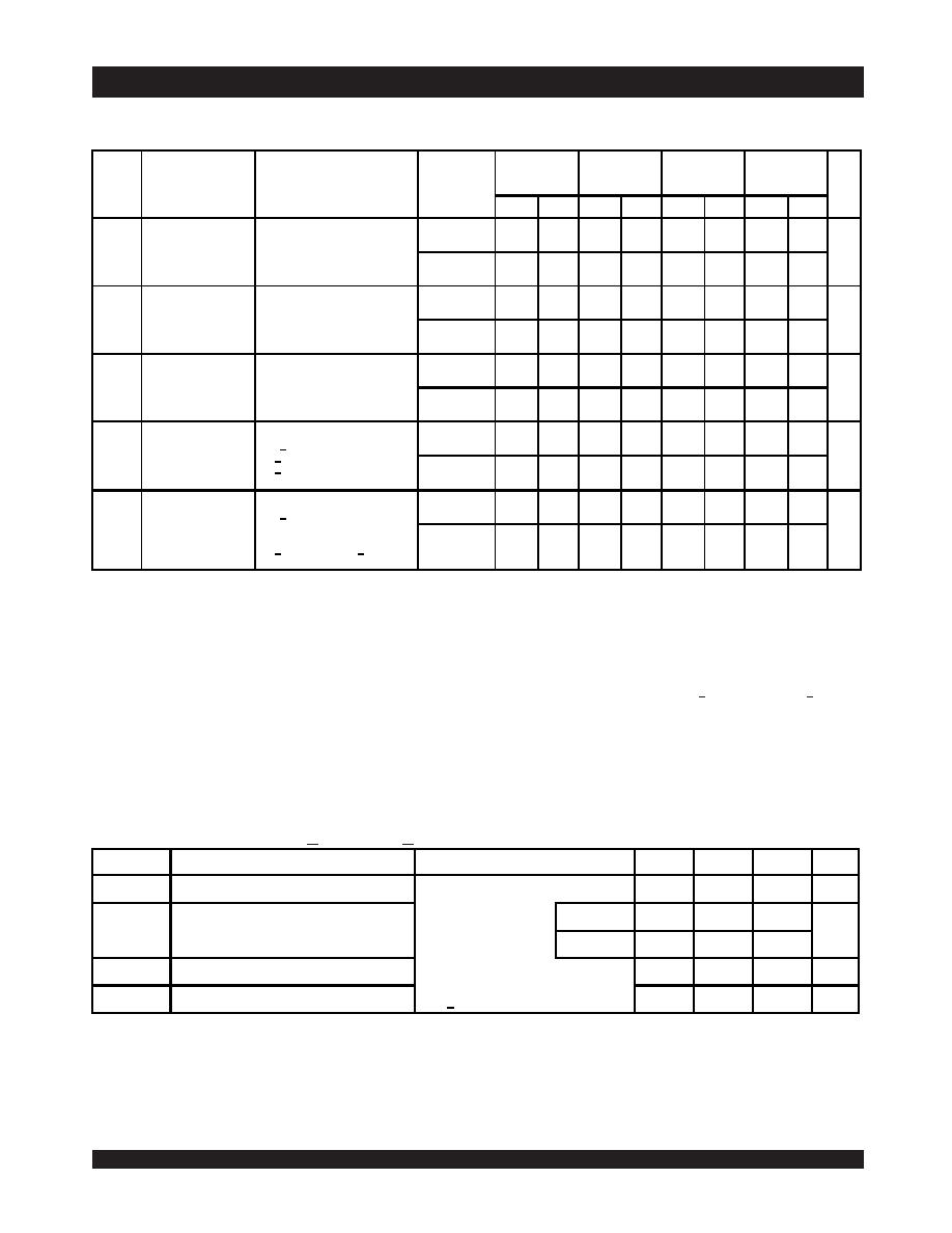
DC Electrical Characteristics Over the Operating
Temperature and Supply Voltage Range(1,2,8)(VCC = 5.0V ± 10%)
Data Retention Characteristics Over All Temperature Ranges
(L Version Only) (VLC < 0.2V, VHC > VCC - 0.2V)
NOTES
1. 'X' in part number indicates power rating (S or L).
2. VCC = 5V, TA = +25°C; guaranteed by device characterization but not production tested.
3. At f = fMAX, address, control lines (except Output Enable), and SCLK are cycling at the maximum frequency read cycle of 1/tRC.
4. f = 0 means no address or control lines change.
5.
SCE may transition, but is Low (SCE=VIL) when clocked in by SCLK.
6.
SCE may be - 0.2V, after it is clocked in, since SCLK=VIH must be clocked in prior to powerdown.
7. If one port is enabled (either
CE or SCE = LOW) then the other port is disabled (SCE or CE = HIGH, respectively). CMOS HIGH > Vcc - 0.2V and LOW < 0.2V, and
TTL HIGH = VIH and LOW = VIL.
8. Industrial temperature: for specific speeds, packages and powers contact your sales office.
NOTES :
1. TA = +25°C, VCC = 2V; guaranteed by device characterization but not production tested.
2. tRC = Read Cycle Time
3. This parameter is guaranteed by device characterization, but is not production tested.
4. To initiate data retention,
SCE = VIH must be clocked in.
70824X20
Com'l Only
70824X25
Com'l Only
70824X35
Com'l &
Military
70824X45
Com'l &
Military
Symbol
Parameter
Test Condition
Version
Typ.(2)
Max.
Typ.(2)
Max.
Typ.(2)
Max.
Typ.(2)
Max.
Unit
ICC
Dynamic Operating
Current
(Both Ports Active)
CEL and CER = VIL,
Outputs Disabled
SCE = VIL(5)
f = fMAX
(3)
COM'L
S
L
180
380
330
170
360
310
160
340
290
155
340
290
mA
MIL &
IND
S
L
____
160
400
340
155
400
340
ISB1
Standby Current
(Both Ports - TTL
Level Inputs)
SCE and CE = VIH(7)
CMD = VIH
f = fMAX(3)
COM'L
S
L
25
70
50
25
70
50
20
70
50
16
70
50
mA
MIL &
IND
S
L
____
20
85
65
16
85
65
ISB2
Standby Current
(One Port - TTL
Level Inputs)
CE or SCE = VIH
Active Port Outputs Disabled,
f=fMAX
(3)
COM'L
S
L
115
260
230
105
250
220
95
240
210
90
240
210
mA
MIL &
IND
S
L
____
95
290
250
90
290
250
ISB3
Full Standby Current
(Both Ports -
CMOS Level Inputs)
Both Ports
CE and
SCE > VCC - 0.2V(6)
VIN > VCC - 0.2V or
VIN < 0.2V,
f = 0(4)
COM'L
S
L
1.0
0.2
15
5
1.0
0.2
15
5
1.0
0.2
15
5
1.0
0.2
15
5
mA
MIL &
IND
S
L
____
1.0
0.2
30
10
1.0
0.2
30
10
ISB4
Full Standby Current
(One Port -
CMOS Level Inputs)
One Port
CE or
SCE > VCC - 0.2V(6,7)
Outputs Disabled (Active Port)
f = fMAX(3)
VIN > VCC - 0.2V or VIN < 0.2V
COM'L
S
L
110
240
200
100
230
190
90
220
180
85
220
180
mA
MIL &
IND
S
L
____
90
260
215
85
260
215
3099 tbl 08
Symbol
Parameter
Test Condition
Min.
Typ.
(1)
Max.
Unit
VDR
VCC for Data Retention
VCC = 2V
2.0
___
V
ICCDR
Data Retention Current
CE = VHC
VIN = VHC or = VLC
MIL. & IND.
___
100
4000
A
COM'L.
___
100
1500
tCDR
(3)
Chip Deselect to Data Retention Time
SCE = VHC(4) when SCLK = u
CMD > VHC
___
V
tR(
3)
Operation Recovery Time
tRC
(2)
___
V
3099 tbl 09
相關(guān)PDF資料 |
PDF描述 |
|---|---|
| 709176001422006 | PCB CONNECTOR |
| 709176001432006 | PCB CONNECTOR |
| 709176001501006 | PCB CONNECTOR |
| 709176001511006 | PCB CONNECTOR |
| 709176001522006 | PCB CONNECTOR |
相關(guān)代理商/技術(shù)參數(shù) |
參數(shù)描述 |
|---|---|
| 70824S20PF | 制造商:Integrated Device Technology Inc 功能描述:SRAM Chip Async Dual 5V 64K-Bit 4K x 16 20ns 80-Pin TQFP Tray |
| 70824S25PF | 制造商:Integrated Device Technology Inc 功能描述:SRAM Chip Async Dual 5V 64K-Bit 4K x 16 25ns 80-Pin TQFP Tray |
| 70825 | 制造商:Gems Sensors & Controls 功能描述:Switches Flow Port Size:1/4" 制造商:Gems Sensors & Controls 功能描述:FLOW SENSOR, 1.5GPM, 69BAR, 1/4" NPT; Pressure Max:69bar; Accuracy %:15%; Port Size:6.35mm; Accuracy:+/-15%; Body Material:Brass; Circuitry:SPST; Connection Size:1/4"; Features:Normally Open at No Flow; Flow Measuring Range:- ;RoHS Compliant: Yes |
| 708250 | 功能描述:固定接線端子 VDFK 4 RoHS:否 制造商:Phoenix Contact 產(chǎn)品:Fixed Terminal Blocks 類型:Wire to Board 節(jié)距:5.08 mm 位置/觸點(diǎn)數(shù)量:2 線規(guī)量程:26-16 電流額定值:13.5 A 電壓額定值:250 V 安裝風(fēng)格:Through Hole 安裝角:Straight 端接類型:Screw 觸點(diǎn)電鍍: |
| 7082534 | 制造商:WIKA INSTRUMENTS 功能描述:Sensor; A-AI-1 Loop Pwrd Ind. for S-10, S-11, A-10 w/DIN 43650, 4-20mA, 2 Wire |
發(fā)布緊急采購,3分鐘左右您將得到回復(fù)。