- 您現(xiàn)在的位置:買賣IC網(wǎng) > PDF目錄373785 > ZL50022 (Zarlink Semiconductor Inc.) Enhanced 4 K Digital Switch with Stratum 4E DPLL PDF資料下載
參數(shù)資料
| 型號: | ZL50022 |
| 廠商: | Zarlink Semiconductor Inc. |
| 英文描述: | Enhanced 4 K Digital Switch with Stratum 4E DPLL |
| 中文描述: | 增強為4 K數(shù)字交換與地層4E條數(shù)字鎖相環(huán) |
| 文件頁數(shù): | 25/121頁 |
| 文件大?。?/td> | 939K |
| 代理商: | ZL50022 |
第1頁第2頁第3頁第4頁第5頁第6頁第7頁第8頁第9頁第10頁第11頁第12頁第13頁第14頁第15頁第16頁第17頁第18頁第19頁第20頁第21頁第22頁第23頁第24頁當(dāng)前第25頁第26頁第27頁第28頁第29頁第30頁第31頁第32頁第33頁第34頁第35頁第36頁第37頁第38頁第39頁第40頁第41頁第42頁第43頁第44頁第45頁第46頁第47頁第48頁第49頁第50頁第51頁第52頁第53頁第54頁第55頁第56頁第57頁第58頁第59頁第60頁第61頁第62頁第63頁第64頁第65頁第66頁第67頁第68頁第69頁第70頁第71頁第72頁第73頁第74頁第75頁第76頁第77頁第78頁第79頁第80頁第81頁第82頁第83頁第84頁第85頁第86頁第87頁第88頁第89頁第90頁第91頁第92頁第93頁第94頁第95頁第96頁第97頁第98頁第99頁第100頁第101頁第102頁第103頁第104頁第105頁第106頁第107頁第108頁第109頁第110頁第111頁第112頁第113頁第114頁第115頁第116頁第117頁第118頁第119頁第120頁第121頁
ZL50022
Data Sheet
25
Zarlink Semiconductor Inc.
The output timing is dependent on the operation mode that is selected. When the device is in Divided Slave mode,
the frequencies on CKo0 - 3 cannot be greater than the input clock, CKi. For example, if the input clock is
8.192 MHz, the CKo2 pin will not produce a valid output clock and the CKo3 pin can only be programmed to output
a 4.096 MHz or 8.192 MHz clock signal. The output clocks CKo4 - 5 will not generate valid outputs unless the
SLV_DPLLEN (bit 13) of the Control Register (CR) is set.
In Master mode there are programmable output frame pulse, FPo3, and clock pins, CKo3 and CKo4. The outputs
from FPo3 and CKo3 are programmed by the CKOFPO3SEL1 - 0 (bits 13 - 12) in the Output Clock and Frame
Pulse Selection (OCFSR) register. The output clock pin, CKo4, is controlled by setting the CKO4SEL (bit 14) in the
OCFSR register.
In Multiplied Slave mode, CKo4 and CKo5 are not available unless SLV_DPLLEN is set in the Control Register. All
other clocks and frame pulses correspond to the timing shown in Table 3 above.
The device also delivers positive or negative output frame pulse and ST-BUS/GCI-Bus output clock formats via the
programming of various bits in the Output Clock and Frame Pulse Selection Register (OCFSR). By default, the
device delivers the negative output clock format. The ZL50022 can also deliver GCI-Bus format output frame
pulses by programming bits of the Output Clock and Frame Pulse Selection Register (OCFSR). As there is a
separate bit setting for each frame pulse output, some of the outputs can be set to operate in ST-BUS mode and
others in GCI-Bus mode.
The following figures describe the usage of the FPO0P, FPO1P, FPO2P, FPO3P, CKO0P, CKO1P, CKO2P, CKO3P,
CKO4P and CKO5P bits to generate the FPo0 - 3 and CKo0 - 5 timing. FPo_OFF2 is configured to provide the
non-offset frame pulse corresponding to the 19.44 MHz clock on CKo5 by setting the FP19EN (bit 10) in the
FPOFF2 register. In this instance, FPo_OFF2 can be labeled as FPo5.
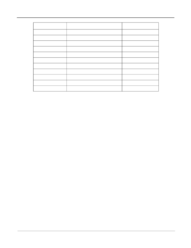
Pin Name
Output Timing Rate
Output Timing Unit
FPo0 pulse width
244
ns
CKo0
4.096
MHz
FPo1 pulse width
122
ns
CKo1
8.192
MHz
FPo2 pulse width
61
ns
CKo2
16.384
MHz
FPo3 pulse width
244, 122, 61 or 30
ns
CKo3
4.096, 8.192, 16.384 or 32.768
MHz
CKo4
1.544 or 2.048
MHz
FPo5 pulse width
51
ns
CKo5
19.44
MHz
Table 3 - Output Timing Generation
相關(guān)PDF資料 |
PDF描述 |
|---|---|
| ZL50022GAC | Enhanced 4 K Digital Switch with Stratum 4E DPLL |
| ZL50022QCC | Enhanced 4 K Digital Switch with Stratum 4E DPLL |
| ZL50023 | Enhanced 4 K Digital Switch |
| ZL50023GAC | Enhanced 4 K Digital Switch |
| ZL50023QCC | Enhanced 4 K Digital Switch |
相關(guān)代理商/技術(shù)參數(shù) |
參數(shù)描述 |
|---|---|
| ZL50022_06 | 制造商:ZARLINK 制造商全稱:Zarlink Semiconductor Inc 功能描述:Enhanced 4 K Digital Switch with Stratum 4E DPLL |
| ZL50022GAC | 制造商:Microsemi Corporation 功能描述:4K WITH RATE CONVERSION AND S4 - Trays 制造商:MICROSEMI CONSUMER MEDICAL PRODUCT GROUP 功能描述:IC TDM SWITCH 4K-CH ENH 256PBGA 制造商:Microsemi Corporation 功能描述:IC TDM SWITCH 4K-CH ENH 256PBGA |
| ZL50022GAG2 | 制造商:Microsemi Corporation 功能描述:SWIT FABRIC 4K X 4K 1.8V/3.3V 256BGA - Trays 制造商:MICROSEMI CONSUMER MEDICAL PRODUCT GROUP 功能描述:IC TDM SWITCH 4K-CH ENH 256PBGA 制造商:Microsemi Corporation 功能描述:IC TDM SWITCH 4K-CH ENH 256PBGA |
| ZL50022QCC | 制造商:Microsemi Corporation 功能描述: 制造商:Microsemi Corporation 功能描述:4K WITH RATE CONVERSION AND S4E DPLL - Trays |
| ZL50022QCG1 | 制造商:Microsemi Corporation 功能描述:PB FREE 4K +RATE CONVERSION & 256L LQFP - Trays 制造商:MICROSEMI CONSUMER MEDICAL PRODUCT GROUP 功能描述:IC TDM SWITCH 4K-CH ENH 256LQFP 制造商:Microsemi Corporation 功能描述:IC TDM SWITCH 4K-CH ENH 256LQFP |
發(fā)布緊急采購,3分鐘左右您將得到回復(fù)。