- 您現(xiàn)在的位置:買賣IC網(wǎng) > PDF目錄1977 > XRT82L24AIV-F (Exar Corporation)IC LIU E1 QAUD 100TQFP PDF資料下載
參數(shù)資料
| 型號(hào): | XRT82L24AIV-F |
| 廠商: | Exar Corporation |
| 文件頁數(shù): | 4/39頁 |
| 文件大小: | 0K |
| 描述: | IC LIU E1 QAUD 100TQFP |
| 標(biāo)準(zhǔn)包裝: | 90 |
| 類型: | 線路接口裝置(LIU) |
| 驅(qū)動(dòng)器/接收器數(shù): | 4/4 |
| 規(guī)程: | E1 |
| 電源電壓: | 3.135 V ~ 3.465 V |
| 安裝類型: | 表面貼裝 |
| 封裝/外殼: | 100-LQFP |
| 供應(yīng)商設(shè)備封裝: | 100-TQFP(14x14) |
| 包裝: | 托盤 |
| 其它名稱: | XRT82L24AIV-F-ND |
第1頁第2頁第3頁當(dāng)前第4頁第5頁第6頁第7頁第8頁第9頁第10頁第11頁第12頁第13頁第14頁第15頁第16頁第17頁第18頁第19頁第20頁第21頁第22頁第23頁第24頁第25頁第26頁第27頁第28頁第29頁第30頁第31頁第32頁第33頁第34頁第35頁第36頁第37頁第38頁第39頁
XRT82L24A
á
QUAD E1 LINE TRANSCEIVER WITH CLOCK RECOVERY AND JITTER ATTENUATOR
REV. 1.1.2
10
SYSTEM-FUNCTIONAL DESCRIPTION
A simplified single channel block diagram of the XRT
82L24A is presented in Figure 1. The XRT 82L24A
consists of four identical transmit and receive chan-
nels for E1(2.048 Mbps) PCM systems. The opera-
tional mode of each channel of the line interface can
be configured by the microprocessor interface (Host
Mode) or by Hardware control.
RECEIVER
At the receiver input, cable attenuated AMI signals
can be coupled to the receiver using a capacitor or a
1:2 transformer. The receive signal first goes through
the equalizer for signal conditioning before being ap-
plied to the data recovery circuit. The data recovery
circuit includes a peak detector which is set typically
at 50% for E1 of the equalizer output peak amplitude
for data slicing. After the data slicers, the digital rep-
resentation of the AMI signals goes to the clock re-
covery circuit for timing recovery and subsequently to
the HDB3 decoder (if selected) before they are output
via the RxPOS/RDATA and RxNEG/LCV pins. The
digital data output can be in dual-rail or single-rail
mode depending on the option selected. Clock and
timing recovery is accomplished by means of a digital
PLL scheme which can tolerate high input jitter and
meets or exceeds the jitter tolerance requirements as
specified in the ITU - G.823 standard.
JITTER ATTENUATOR
To reduce jitter in the transmit line signal or recovered
clock and data signals, a crystal-less jitter attenuator
with a 32x2 bit or 64x2 bit FIFO is provided for each
channel. The jitter attenuator can be configured to op-
erate in either the transmit or receive path, or it can
be disabled through Host or Hardware Mode control.
The jitter attenuator design is based on a digital
scheme that uses the MCLK signal as a reference in-
put. No other high frequency clock is necessary. With
the jitter attenuator selected, the typical throughput
delay is 16 bits for a 32 bit FIFO depth or 32 bit for a
64 bit FIFO depth. The design of the jitter attenuator
is such that if the write and read pointers of the FIFO
are within two bits of overflowing or underflowing, the
bandwidth of the jitter attenuator is automatically wid-
ened in order to permit the “Jitter Attenuator” PLL to
track the short term input jitter to avoid data corrup-
tion. When this situation occurs, the jitter attenuator
will not attenuate input jitter until the read/write point-
er's position is outside the two bit window. Under nor-
mal condition, the jitter transfer characteristic meets
the narrow bandwidth requirement as specified in
ITU- G.736 and ITU- I.431standards.
GAPPED CLOCK (JA MUST BE ENABLED IN
THE TRANSMIT PATH)
The XRT82L24A LIU is ideal for multiplexer or
mapper applications where the network data crosses
multiple timing domains. As the higher data rates are
de-multiplexed down to T1 or E1 data, stuffing bits
are removed which can leave gaps in the incoming
data stream. If the jitter attenuator is enabled in the
transmit path, the 32-Bit or 64-Bit FIFO is used to
smooth the gapped clock into a steady T1 or E1
output. The maximum gap width of the XRT82L24A
is shown in Table 1.
NOTE: If the LIU is used in a loop timing system, the jitter
attenuator should be enabled in the receive path.
HDB3/AMI DECODER
The decoder function is only active if the chip has
been configured to operate in the single-rail mode.
When the single-rail mode is selected, the receive
line signal will be decoded according to HDB3 rules
for E1. Further, any bipolar violation of the HDB3 line
coding scheme will be flagged as a Line Code Viola-
tion via the LCV output pin. The LCV output pin will
be pulsed high for one RxClk cycle for each line code
violation that is detected. Excessive number of zeros
in the receive data stream are also flagged as a line
code violation via the same output pin. If AMI decod-
ing is selected in single-rail mode operation, every bi-
polar violation in the receive data stream is reported
as error at the LCV pin.
RECEIVER LOSS OF SIGNAL (LOS)
The receiver loss of signal monitoring function is im-
plemented using both analog and digital detection
schemes compatible with ITU G.775 requirements.
When the amplitude of the E1line signal at RTIP/
RRING drops 16dB (typical) below the 0dB nominal
level the digital circuit is activated to parse through
and check for 32 consecutive zeros before LOS is as-
serted, to indicate loss of input signal. The number of
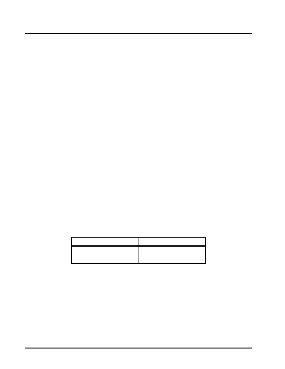
TABLE 1: MAXIMUM GAP WIDTH FOR MULTIPLEXER/MAPPER APPLICATIONS
FIFO DEPTH
MAXIMUM GAP WIDTH
32-Bit
20 UI
64-Bit
50 UI
相關(guān)PDF資料 |
PDF描述 |
|---|---|
| XRT83D10IW | IC LIU T1/E1 SGL 28SOJ |
| XRT83L30IV-F | IC LIU LH/SH T1/E1 SGL 64TQFP |
| XRT83L314IB-L | IC LIU T1/E1/J1 14CH 304TBGA |
| XRT83L34IV-F | IC LIU T1/E1/J1 QUAD 128TQFP |
| XRT83L38IB-F | IC LIU T1/E1/J1 OCTAL 225BGA |
相關(guān)代理商/技術(shù)參數(shù) |
參數(shù)描述 |
|---|---|
| XRT82L24ES | 功能描述:界面開發(fā)工具 Evaluation Board for XRT82L24 Series RoHS:否 制造商:Bourns 產(chǎn)品:Evaluation Boards 類型:RS-485 工具用于評(píng)估:ADM3485E 接口類型:RS-485 工作電源電壓:3.3 V |
| XRT82L24IV | 制造商:EXAR 制造商全稱:EXAR 功能描述:QUAD E1 LINE TRANSCEIVER WITH CLOCK RECOVERY AND JITTER ATTENUATOR |
| XRT82L34IV | 制造商:未知廠家 制造商全稱:未知廠家 功能描述:Interface IC |
| XRT83D10 | 制造商:EXAR 制造商全稱:EXAR 功能描述:SINGLE CHANNEL DS1/CEPT LINE INTERFACE UNIT |
| XRT83D10ES | 功能描述:外圍驅(qū)動(dòng)器與原件 - PCI 1 CHT1/E1LIUSH RoHS:否 制造商:PLX Technology 工作電源電壓: 最大工作溫度: 安裝風(fēng)格:SMD/SMT 封裝 / 箱體:FCBGA-1156 封裝:Tray |
發(fā)布緊急采購,3分鐘左右您將得到回復(fù)。