- 您現(xiàn)在的位置:買賣IC網(wǎng) > PDF目錄371305 > XA-H3 (NXP Semiconductors N.V.) CMOS 16-bit highly integrated microcontroller PDF資料下載
參數(shù)資料
| 型號(hào): | XA-H3 |
| 廠商: | NXP Semiconductors N.V. |
| 英文描述: | CMOS 16-bit highly integrated microcontroller |
| 中文描述: | 的CMOS 16位高度集成的微控制器 |
| 文件頁(yè)數(shù): | 29/36頁(yè) |
| 文件大小: | 183K |
| 代理商: | XA-H3 |
第1頁(yè)第2頁(yè)第3頁(yè)第4頁(yè)第5頁(yè)第6頁(yè)第7頁(yè)第8頁(yè)第9頁(yè)第10頁(yè)第11頁(yè)第12頁(yè)第13頁(yè)第14頁(yè)第15頁(yè)第16頁(yè)第17頁(yè)第18頁(yè)第19頁(yè)第20頁(yè)第21頁(yè)第22頁(yè)第23頁(yè)第24頁(yè)第25頁(yè)第26頁(yè)第27頁(yè)第28頁(yè)當(dāng)前第29頁(yè)第30頁(yè)第31頁(yè)第32頁(yè)第33頁(yè)第34頁(yè)第35頁(yè)第36頁(yè)

Philips Semiconductors
Preliminary specification
XA-H3
CMOS 16-bit highly integrated microcontroller
1999 Sep 24
29
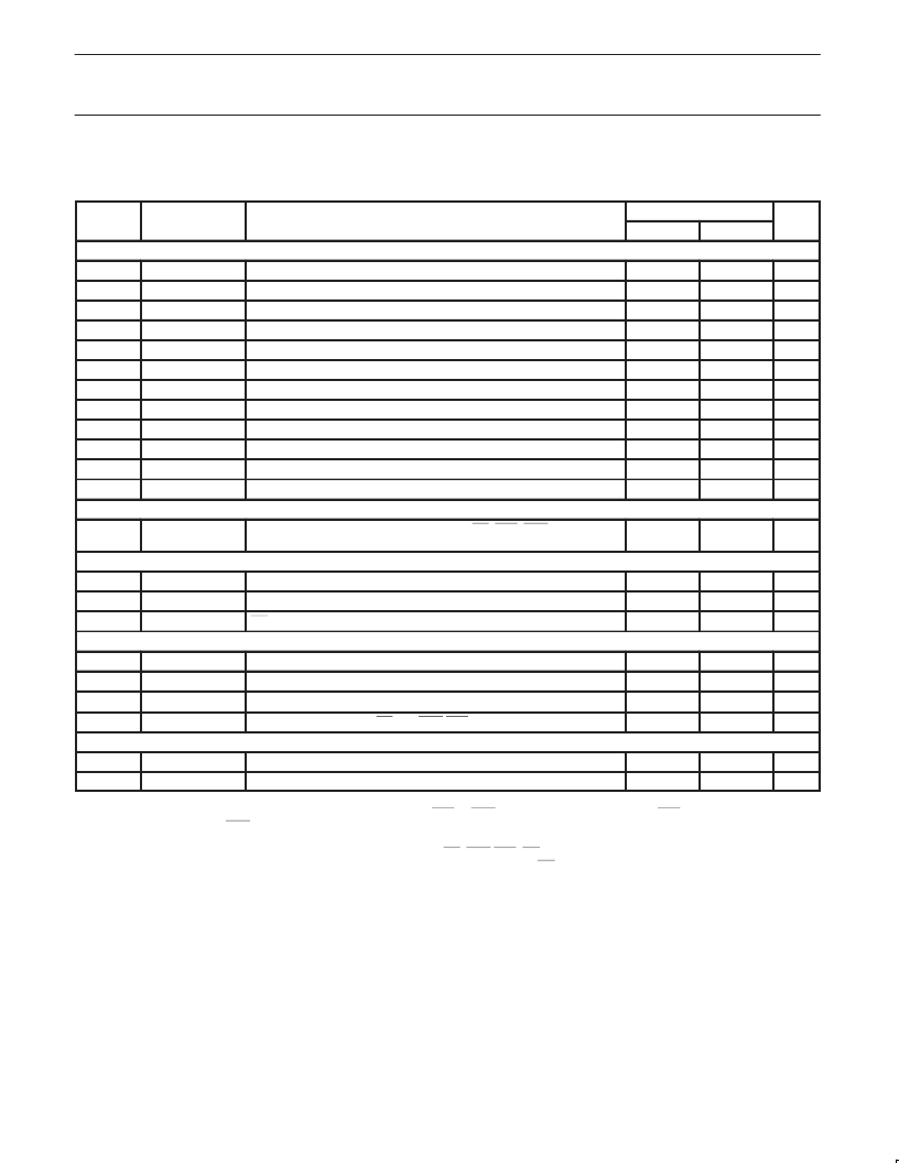
AC ELECTRICAL CHARACTERISTICS (3.3 V +/–10%)
Vdd = 3.3 V +/– 10%; T
amb
= –40
°
C to +85
°
C ( industrial )
Symbol
Fig re
Figure
Parameter
Limits
Unit
Min
Max
All Cycles
F
C
t
C
System Clock (internally called CClk) Frequency
0
30
MHz
13
System Clock Period = 1/FC
33.33
–
ns
t
CHCX
t
CLCX
t
CLCH
t
CHCL
t
AVSL
t
CHAH
t
CHAV
t
CHSH
t
CHSL
t
CODH
13
XTALIN High Time
t
C
* 0.5
t
C
* 0.4
–
–
ns
13
XTALIN Low Time
–
ns
13
XTALIN Rise Time
5
ns
13
XTALIN Fall Time
–
5
ns
All
Address Valid to Strobe low
Address hold after CLKOUT rising edge
7
t
C
– 21
1
–
ns
All
–
ns
All
Delay from CLKOUT rising edge to address valid
Delay from CLKOUT rising edge to Strobe High
7
Delay from CLKOUT rising edge to Strobe Low
7
–
30
ns
All
1
28
ns
All
1
25
ns
14
ClkOut Duty Cycle High (into 40 pF max.)
t
CHCX
–7
t
CHCX
+3
ns
Data Read Only
t
AHDR
10
Address hold (A19 – A1 only, not A0) after CS, BLE, BHE rise at end
of Data Read Cycle (not code fetch)
t
C
– 12
–
ns
Data Read and Instruction Fetch Cycles
t
DIS
t
DIH
t
OHDE
7, 8, 10, 11
Data In Valid setup to ClkOut rising edge
Data In Valid hold after ClkOut rising edge
2
32
–
ns
7, 8, 10, 11
0
–
ns
10
OE high to XA Data Bus Driver Enable
t
C
– 19
–
ns
Write Cycles
t
CHDV
t
DVSL
t
SHAH
t
SHDH
9
Clock High to Data Valid
–
30
ns
12
Data Valid prior to Strobe Low
t
C
– 23
t
C
– 25
t
C
– 25
–
ns
9, 12
Minimum Address Hold Time after strobe goes inactive
–
ns
9, 12
Data hold after strobes (CS and BHE/BLE) high
–
ns
Wait Input
t
WS
t
WH
15
WAIT setup (stable high or low)prior to CLKOUT rising edge
25
–
ns
15
WAIT hold (stable high or low) after CLKOUT rising edge
0
–
ns
NOTE:
1. On a 16-bit bus, if only one byte is being written, then only one of BLE or BHE will go active. On an 8-bit bus, BLE goes active for all (odd or
even address) accesses. BHE will not go active during any accesses on an 8-bit bus.
2. The bus timing is designed to make meeting hold time very straightforward without glue logic. On all reads and fetches, in order to meet hold
time, the slave should hold data valid on the bus until the earliest of CS, BHE/BLE, OE, goes high (inactive), or until the address changes.
3. To avoid 3-State fights during read cycles and fetch cycles, do not drive data bus until OE goes active
4.
WARNING:
ClkOut is specified at 40 pF max. More than 40 pf on ClkOut may significantly degrade the ClkOut waveform. Load capacitance
for all outputs (except ClkOut) = 80 pF.
5. Not all combinations of bus timing configuration values result in valid bus cycles. Please refer to the XA-H3 User Manualfor details.
6. When code is being fetched on the external bus, a burst mode fetch is used. This burst can be from 2 to 16 bytes long. On a 16-bit bus,
A3 – A1 are incremented for each new word of the burst. On an 8-bit bus, A3 – A0 are incremented for each new byte of the burst code fetch.
7. The MIN value for this parameter is guaranteed by design and is not tested in production to the specified limit. In those cases where a
maximum value is specified in the table for this parameter, it is tested.
相關(guān)PDF資料 |
PDF描述 |
|---|---|
| XA-H4 | Single-chip 16-bit microcontroller |
| XACA04SPEC0304 | CONTROL STATION 4WAY |
| XACA06SPEC0305 | CONTROL STATION 6WAY |
| XACA215 | FERNSTEUEREINHEIT |
| XALB222 | WIPPSCHALTER ZB2 STEUERGEHAEUSE TASTEN 2 |
相關(guān)代理商/技術(shù)參數(shù) |
參數(shù)描述 |
|---|---|
| XA-H4 | 制造商:PHILIPS 制造商全稱:NXP Semiconductors 功能描述:Single-chip 16-bit microcontroller |
| XAI.50V2200 | 制造商:Xicon Passive Components 功能描述: |
| XAIR1-3402-101B | 制造商:Advantech Co Ltd 功能描述:CARRIER BOARD, AIR PRODUCTS 3402-101B3 - Bulk |
| XAIR1-3402-CARTON | 制造商:Advantech Co Ltd 功能描述:D-AIR01-SOM7562-01 - OUTER CARTON - Bulk |
| XAITD-100 | 制造商:RHOMBUS-IND 制造商全稱:Rhombus Industries Inc. 功能描述:XAITD Series FAST / TTL Buffered 10-Tap Delay Modules |
發(fā)布緊急采購(gòu),3分鐘左右您將得到回復(fù)。