- 您現(xiàn)在的位置:買賣IC網(wǎng) > PDF目錄203637 > W9425G8DH-6 (WINBOND ELECTRONICS CORP) 32M X 8 DDR DRAM, 0.7 ns, PDSO66 PDF資料下載
參數(shù)資料
| 型號: | W9425G8DH-6 |
| 廠商: | WINBOND ELECTRONICS CORP |
| 元件分類: | DRAM |
| 英文描述: | 32M X 8 DDR DRAM, 0.7 ns, PDSO66 |
| 封裝: | 0.400 INCH, 0.65 MM PITCH, ROHS COMPLIANT, TSOP2-66 |
| 文件頁數(shù): | 18/53頁 |
| 文件大小: | 1920K |
| 代理商: | W9425G8DH-6 |
第1頁第2頁第3頁第4頁第5頁第6頁第7頁第8頁第9頁第10頁第11頁第12頁第13頁第14頁第15頁第16頁第17頁當(dāng)前第18頁第19頁第20頁第21頁第22頁第23頁第24頁第25頁第26頁第27頁第28頁第29頁第30頁第31頁第32頁第33頁第34頁第35頁第36頁第37頁第38頁第39頁第40頁第41頁第42頁第43頁第44頁第45頁第46頁第47頁第48頁第49頁第50頁第51頁第52頁第53頁
W9425G8DH
Publication Release Date: Nov. 20, 2007
- 25 -
Revision A4
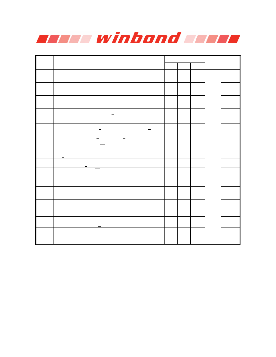
9.5 DC Characteristics
MAX.
SYM.
PARAMETER
-5
-6
-75
UNIT
NOTES
IDD0
Operating current: One Bank Active-Precharge; tRC = tRC min; tCK
= tCK min; DQ, DM and DQS inputs changing twice per clock
cycle; Address and control inputs changing once per clock cycle
110
7
IDD1
Operating current: One Bank Active-Read-Precharge; Burst = 2;
tRC = tRC min; CL = 3; tCK = tCK min; IOUT = 0 mA; Address and
control inputs changing once per clock cycle.
150
7, 9
IDD2P
Precharge Power Down standby current: All Banks Idle; Power
down mode; CKE < VIL max; tCK = tCK min; Vin = VREF for DQ,
DQS and DM
20
IDD2F
Idle floating standby current: CS > VIH min; All Banks Idle; CKE
> VIH min; Address and other control inputs changing once per
clock cycle; Vin = VREF for DQ, DQS and DM
45
40
7
IDD2N
Idle standby current: CS > VIH min; All Banks Idle; CKE > VIH
min; tCK = tCK min; Address and other control inputs changing
once per clock cycle; Vin > VIH min or Vin < VIL max for DQ, DQS
and DM
45
40
7
IDD2Q
Idle quiet standby current: CS > VIH min; All Banks Idle; CKE >
VIH min; tCK = tCK min; Address and other control inputs stable;
Vin > VREF for DQ, DQS and DM
40
35
7
IDD3P
Active Power Down standby current: One Bank Active; Power
down mode; CKE < VIL max; tCK = tCK min
20
IDD3N
Active standby current: CS > VIH min; CKE > VIH min; One Bank
Active-Precharge; tRC = tRAS max; tCK = tCK min; DQ, DM and
DQS inputs changing twice per clock cycle; Address and other
control inputs changing once per clock cycle
70
65
7
IDD4R
Operating current: Burst = 2; Reads; Continuous burst; One Bank
Active; Address and control inputs changing once per clock cycle;
CL=3; tCK = tCK min; IOUT = 0mA
180
170
160
7, 9
IDD4W
Operating current: Burst = 2; Write; Continuous burst; One Bank
Active; Address and control inputs changing once per clock cycle;
CL = 3; tCK = tCK min; DQ, DM and DQS inputs changing twice per
clock cycle
180
170
160
7
IDD5
Auto Refresh current: tRC = tRFC min
190
7
IDD6
Self Refresh current: CKE < 0.2V
3
IDD7
Random Read current: 4 Banks Active Read with activate every
20nS, Auto-Precharge Read every 20 nS; Burst = 4; tRCD = 3; IOUT
= 0mA; DQ, DM and DQS inputs changing twice per clock cycle;
Address changing once per clock cycle
300
mA
相關(guān)PDF資料 |
PDF描述 |
|---|---|
| W946432AD-6 | 2M X 32 DDR DRAM, 0.1 ns, PQFP100 |
| W947D6HBHX6E | 8M X 16 DDR DRAM, 5 ns, PBGA60 |
| W9602BB | PUSHBUTTON SWITCH, SPST, MOMENTARY, 10A, 28VDC, PANEL MOUNT-THREADED |
| W9605BB | PUSHBUTTON SWITCH, SPST, MOMENTARY, 10A, 28VDC, PANEL MOUNT-THREADED |
| W9606BB | PUSHBUTTON SWITCH, SPDT, MOMENTARY, 10A, 28VDC, PANEL MOUNT-THREADED |
相關(guān)代理商/技術(shù)參數(shù) |
參數(shù)描述 |
|---|---|
| W9425G8EH | 制造商:WINBOND 制造商全稱:Winbond 功能描述:8M × 4 BANKS × 8 BITS DDR SDRAM |
| W946432AD | 制造商:WINBOND 制造商全稱:Winbond 功能描述:512K X 4 BANKS X 32 BITS DDR SDRAM |
| W9464G6IB | 制造商:WINBOND 制造商全稱:Winbond 功能描述:1M × 4 BANKS × 16 BITS DDR SDRAM |
| W9464G6IH | 制造商:WINBOND 制造商全稱:Winbond 功能描述:1M ?? 4 BANKS ?? 16 BITS DDR SDRAM |
| W9464G6JH | 制造商:WINBOND 制造商全稱:Winbond 功能描述:1M ? 4 BANKS ? 16 BITS DDR SDRAM |
發(fā)布緊急采購,3分鐘左右您將得到回復(fù)。