- 您現(xiàn)在的位置:買賣IC網(wǎng) > PDF目錄199495 > TSPC860SRMZPU40D4 (E2V TECHNOLOGIES PLC) 32-BIT, 40 MHz, RISC PROCESSOR, PBGA357 PDF資料下載
參數(shù)資料
| 型號: | TSPC860SRMZPU40D4 |
| 廠商: | E2V TECHNOLOGIES PLC |
| 元件分類: | 微控制器/微處理器 |
| 英文描述: | 32-BIT, 40 MHz, RISC PROCESSOR, PBGA357 |
| 封裝: | PLASTIC, BGA-357 |
| 文件頁數(shù): | 18/90頁 |
| 文件大?。?/td> | 2351K |
| 代理商: | TSPC860SRMZPU40D4 |
第1頁第2頁第3頁第4頁第5頁第6頁第7頁第8頁第9頁第10頁第11頁第12頁第13頁第14頁第15頁第16頁第17頁當前第18頁第19頁第20頁第21頁第22頁第23頁第24頁第25頁第26頁第27頁第28頁第29頁第30頁第31頁第32頁第33頁第34頁第35頁第36頁第37頁第38頁第39頁第40頁第41頁第42頁第43頁第44頁第45頁第46頁第47頁第48頁第49頁第50頁第51頁第52頁第53頁第54頁第55頁第56頁第57頁第58頁第59頁第60頁第61頁第62頁第63頁第64頁第65頁第66頁第67頁第68頁第69頁第70頁第71頁第72頁第73頁第74頁第75頁第76頁第77頁第78頁第79頁第80頁第81頁第82頁第83頁第84頁第85頁第86頁第87頁第88頁第89頁第90頁
25
TSPC860
2129A–HIREL–08/02
Active Pull-up Buffers
Active pull-up buffers are a special variety of bidirectional three-state buffer with the fol-
lowing properties:
When enabled as an output and driving low, they behave as normal output drivers
(that is, the pin is constantly driven low).
When enabled as an output and driving high, drive high until an internal detection
circuit determines that the output has reached the logic high threshold and then stop
driving (that is, the pin switches to high-impedance).
When disabled as an output or functioning as an input, it should not be driven.
Due to the behavior of the buffer when being driven high, a pull-up resistor is required
externally to function as a ‘bus keep’ for these shared signals in periods when no drivers
are active and to keep the buffer from oscillating when the buffer is driving high,
because if the voltage ever dips below the logic high threshold while the buffer is
enabled as an output, the buffer will reactivate. Further, external logic must not attempt
to drive these signals low while active pull-up buffers are enabled as outputs, because
the buffers will reactivate and drive high, resulting in a buffer fight and possible damage
to the TSPC860, to the system, or to both.
Figure 6 compares three-state buffers and active pull-up buffers graphically in general
terms. It makes no implication as to which edges trigger which events for any particular
signal.
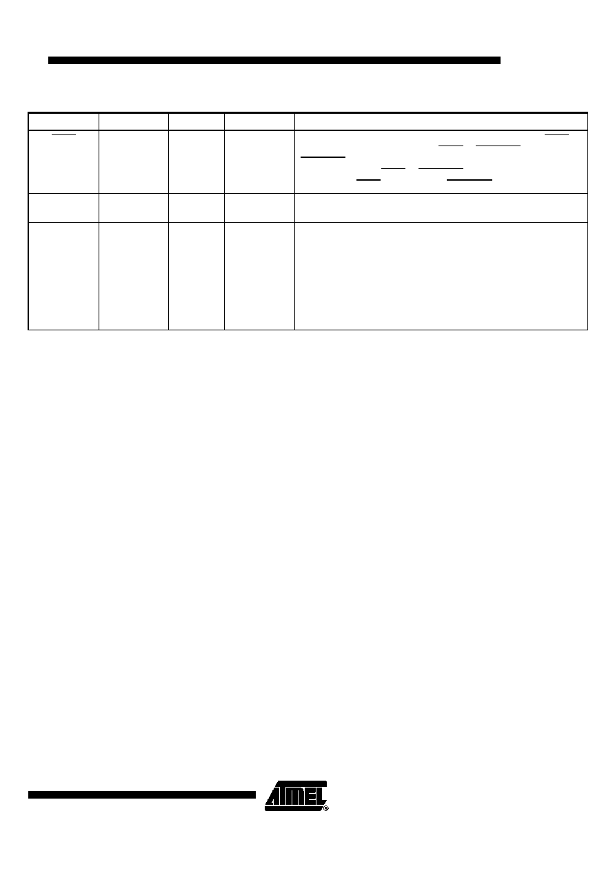
TRST
Pulled up
G19
Input
Reset for the scan chain logic. If JTAG is not used, connect TRST to
ground. If JTAG is used, connect TRST to PORESET. In case
PORESET logic is powered by the keep-alive power supply
(KAPWR), connect TRST to PORESET through a diode (anode
connected to TRST and cathode to PORESET).
SPARE[1-4]
Hi-Z
B7, H18,
V15, H4
No-connect
Spare signals — Not used on current chip revisions. Leave
unconnected.
Power Supply
See
Figure 4
Power
V
DDL — Power supply of the internal logic.
V
DDH — Power supply of the I/O buffers and certain parts of the clock
control.
V
DDSYN — Power supply of the PLL circuitry.
KAPWR — Power supply of the internal OSCM, RTC, PIT, DEC, and
TB.
V
SS — Ground for circuits, except for the PLL circuitry.
V
SSSYN, VSSSYN1 — Ground for the PLL circuitry.
Table 1. Signal Descriptions (Continued)
Name
Reset
Number
Type
Description
相關PDF資料 |
PDF描述 |
|---|---|
| TSPC860SRMZPU50D4 | 32-BIT, 50 MHz, RISC PROCESSOR, PBGA357 |
| TSPD11CGVRA0 | PUSHBUTTON SWITCH, SPST, MOMENTARY, 0.02A, 20VDC, THROUGH HOLE-RIGHT ANGLE |
| 2-1437573-9 | PUSHBUTTON SWITCH, SPDT, MOMENTARY, 0.02A, 20VDC, SURFACE MOUNT-RIGHT ANGLE |
| 3-1437573-4 | PUSHBUTTON SWITCH, SPST, MOMENTARY, 0.02A, 20VDC, THROUGH HOLE-RIGHT ANGLE |
| TSPF5400AS21 | 5 mm, 1 ELEMENT, INFRARED LED, 870 nm |
相關代理商/技術參數(shù) |
參數(shù)描述 |
|---|---|
| TSPC860SRMZQU66D | 制造商:e2v technologies 功能描述:MPU RISC 32BIT 66MHZ 3.3V 357BGA - Trays |
| TSPC860SRVZQU66D | 制造商:e2v technologies 功能描述:TSPC860SRVZQU66D - Trays |
| TSPC860XRMZPU66D | 制造商:ATMEL 制造商全稱:ATMEL Corporation 功能描述:Integrated Communication Processor |
| TSPC860XRMZQU66D | 制造商:ATMEL 制造商全稱:ATMEL Corporation 功能描述:Integrated Communication Processor |
| TSPC860XRVZPU66D | 制造商:ATMEL 制造商全稱:ATMEL Corporation 功能描述:Integrated Communication Processor |
發(fā)布緊急采購,3分鐘左右您將得到回復。