- 您現(xiàn)在的位置:買賣IC網(wǎng) > PDF目錄300038 > TMS320LF2407APGEA (TEXAS INSTRUMENTS INC) 16-BIT, 20 MHz, OTHER DSP, PQFP144 PDF資料下載
參數(shù)資料
| 型號(hào): | TMS320LF2407APGEA |
| 廠商: | TEXAS INSTRUMENTS INC |
| 元件分類: | 數(shù)字信號(hào)處理 |
| 英文描述: | 16-BIT, 20 MHz, OTHER DSP, PQFP144 |
| 封裝: | GREEN, PLASTIC, LQFP-144 |
| 文件頁數(shù): | 45/134頁 |
| 文件大?。?/td> | 1724K |
| 代理商: | TMS320LF2407APGEA |
第1頁第2頁第3頁第4頁第5頁第6頁第7頁第8頁第9頁第10頁第11頁第12頁第13頁第14頁第15頁第16頁第17頁第18頁第19頁第20頁第21頁第22頁第23頁第24頁第25頁第26頁第27頁第28頁第29頁第30頁第31頁第32頁第33頁第34頁第35頁第36頁第37頁第38頁第39頁第40頁第41頁第42頁第43頁第44頁當(dāng)前第45頁第46頁第47頁第48頁第49頁第50頁第51頁第52頁第53頁第54頁第55頁第56頁第57頁第58頁第59頁第60頁第61頁第62頁第63頁第64頁第65頁第66頁第67頁第68頁第69頁第70頁第71頁第72頁第73頁第74頁第75頁第76頁第77頁第78頁第79頁第80頁第81頁第82頁第83頁第84頁第85頁第86頁第87頁第88頁第89頁第90頁第91頁第92頁第93頁第94頁第95頁第96頁第97頁第98頁第99頁第100頁第101頁第102頁第103頁第104頁第105頁第106頁第107頁第108頁第109頁第110頁第111頁第112頁第113頁第114頁第115頁第116頁第117頁第118頁第119頁第120頁第121頁第122頁第123頁第124頁第125頁第126頁第127頁第128頁第129頁第130頁第131頁第132頁第133頁第134頁
TMS320LF2407A,TMS320LF2406A,TMS320LF2403A,TMS320LF2402A
TMS320LC2406A,TMS320LC2404A,TMS320LC2403A,TMS320LC2402A
DSP CONTROLLERS
SPRS145L JULY 2000 REVISED SEPTEMBER 2007
18
POST OFFICE BOX 1443
HOUSTON, TEXAS 772511443
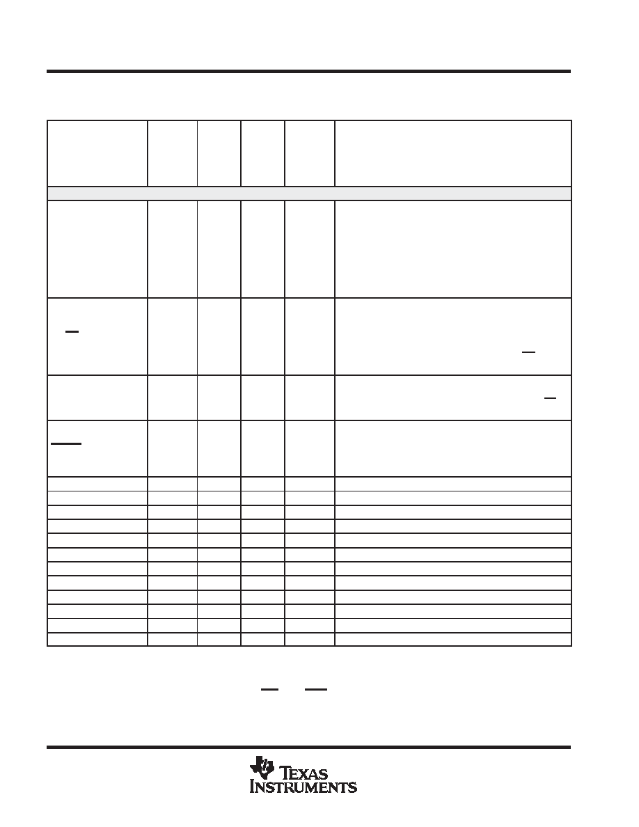
pin functions (continued)
Table 2. LF240xA and LC240xA Pin List and Package Options (Continued)
PIN NAME
LF2407A
(144-PGE)
2406A
(100-PZ)
LC2404A
(100-PZ)
2403A,
LC2402A
(64-PAG)
and
2402A
(64-PG)
DESCRIPTION
ADDRESS, DATA, AND MEMORY CONTROL SIGNALS (CONTINUED)
READY
120
READY is pulled low to add wait states for external accesses.
READY indicates that an external device is prepared for a bus
transaction to be completed. If the device is not ready, it pulls the
READY pin low. The processor waits one cycle and checks
READY
again.
Note
that
the
processor
performs
READY-detection if at least one software wait state is
programmed. To meet the external READY timing parameters,
the wait-state generator control register (WSGR) should be
programmed for at least one wait state.
(
↑)
MP/MC
118
Microprocessor/Microcomputer mode select. If this pin is low
during reset, the device is put in microcomputer mode and
program execution begins at 0000h of internal program memory
(Flash EEPROM). A high value during reset puts the device in
microprocessor mode and program execution begins at 0000h
of external program memory. This line sets the MP/MC bit (bit 2
in the SCSR2 register).
(
↓)
ENA_144
122
Active high to enable external interface signals. If pulled low, the
2407A behaves like the 2406A/2403A/2402A—i.e., it has no
external memory and generates an illegal address if DS is
asserted. This pin has an internal pulldown.
(
↓)
VIS_OE
97
Visibility output enable (active when data bus is output). This pin
is active (low) whenever the external data bus is driving as an
output during visibility mode. Can be used by external decode
logic to prevent data bus contention while running in visibility
mode.
A0
80
Bit 0 of the 16-bit address bus
A1
78
Bit 1 of the 16-bit address bus
A2
74
Bit 2 of the 16-bit address bus
A3
71
Bit 3 of the 16-bit address bus
A4
68
Bit 4 of the 16-bit address bus
A5
64
Bit 5 of the 16-bit address bus
A6
61
Bit 6 of the 16-bit address bus
A7
57
Bit 7 of the 16-bit address bus
A8
53
Bit 8 of the 16-bit address bus
A9
51
Bit 9 of the 16-bit address bus
A10
48
Bit 10 of the 16-bit address bus
A11
45
Bit 11 of the 16-bit address bus
Bold, italicized pin names indicate pin function after reset.
GPIO General-purpose input/output pin. All GPIOs come up as input after reset.
§ It is highly recommended that VCCA be isolated from the digital supply voltage (and VSSA from digital ground) to maintain the specified accuracy
and improve the noise immunity of the ADC.
Only when all of the following conditions are met: EMU1/OFF is low, TRST is low, and EMU0 is high
# No power supply pin (VDD, VDDO, VCCA, VSS, or VSSO) should be left unconnected. All power supply pins must be connected appropriately for
proper device operation.
LEGEND:
↑ Internal pullup
↓ Internal pulldown
(Typical active pullup/pulldown value is
±16 A.)
相關(guān)PDF資料 |
PDF描述 |
|---|---|
| TMS426409AP-60DJ | 4M X 4 EDO DRAM, 60 ns, PDSO24 |
| TMS426809AP-70DGC | 2M X 8 EDO DRAM, 70 ns, PDSO28 |
| TMS44400DJ-80 | 1M X 4 FAST PAGE DRAM, 80 ns, PDSO20 |
| TMS470R1B768PGEQR | 32-BIT, FLASH, 60 MHz, RISC MICROCONTROLLER, PQFP144 |
| TMS4C1050-4DJL | 256K X 4 OTHER FIFO, PDSO20 |
相關(guān)代理商/技術(shù)參數(shù) |
參數(shù)描述 |
|---|---|
| TMS320LF2407APGEA | 制造商:Texas Instruments 功能描述:16BIT DSP FLASH SMD 320LF2407 |
| TMS320LF2407APGEG4 | 功能描述:數(shù)字信號(hào)處理器和控制器 - DSP, DSC 16-Bit Fixed-Pt DSP with Flash RoHS:否 制造商:Microchip Technology 核心:dsPIC 數(shù)據(jù)總線寬度:16 bit 程序存儲(chǔ)器大小:16 KB 數(shù)據(jù) RAM 大小:2 KB 最大時(shí)鐘頻率:40 MHz 可編程輸入/輸出端數(shù)量:35 定時(shí)器數(shù)量:3 設(shè)備每秒兆指令數(shù):50 MIPs 工作電源電壓:3.3 V 最大工作溫度:+ 85 C 封裝 / 箱體:TQFP-44 安裝風(fēng)格:SMD/SMT |
| TMS320LF2407APGES | 功能描述:數(shù)字信號(hào)處理器和控制器 - DSP, DSC 16-Bit Univ Bus Drv With 3-State Outputs RoHS:否 制造商:Microchip Technology 核心:dsPIC 數(shù)據(jù)總線寬度:16 bit 程序存儲(chǔ)器大小:16 KB 數(shù)據(jù) RAM 大小:2 KB 最大時(shí)鐘頻率:40 MHz 可編程輸入/輸出端數(shù)量:35 定時(shí)器數(shù)量:3 設(shè)備每秒兆指令數(shù):50 MIPs 工作電源電壓:3.3 V 最大工作溫度:+ 85 C 封裝 / 箱體:TQFP-44 安裝風(fēng)格:SMD/SMT |
| TMS320LF2407PGES | 制造商:Rochester Electronics LLC 功能描述:- Bulk |
| TMS320M640AGNZ4 | 制造商:Texas Instruments 功能描述:TMS320DM640 548PIN FCBGA PG2.0 - Trays |
發(fā)布緊急采購,3分鐘左右您將得到回復(fù)。