- 您現(xiàn)在的位置:買賣IC網(wǎng) > PDF目錄385920 > TDC2302B (Texas Instruments, Inc.) STS-3/STM-1 Line Interface(STS-3/STM-1線性接口) PDF資料下載
參數(shù)資料
| 型號(hào): | TDC2302B |
| 廠商: | Texas Instruments, Inc. |
| 英文描述: | STS-3/STM-1 Line Interface(STS-3/STM-1線性接口) |
| 中文描述: | STS-3/STM-1線路接口(STS-3/STM-1線性接口) |
| 文件頁數(shù): | 5/17頁 |
| 文件大小: | 390K |
| 代理商: | TDC2302B |
TDC2302B
STS-3/STM-1 LINE INTERFACE
SDNS002 – SEPTEMBER 1992 – REVISED JUNE 1993
POST OFFICE BOX 655303
DALLAS, TEXAS 75265
5
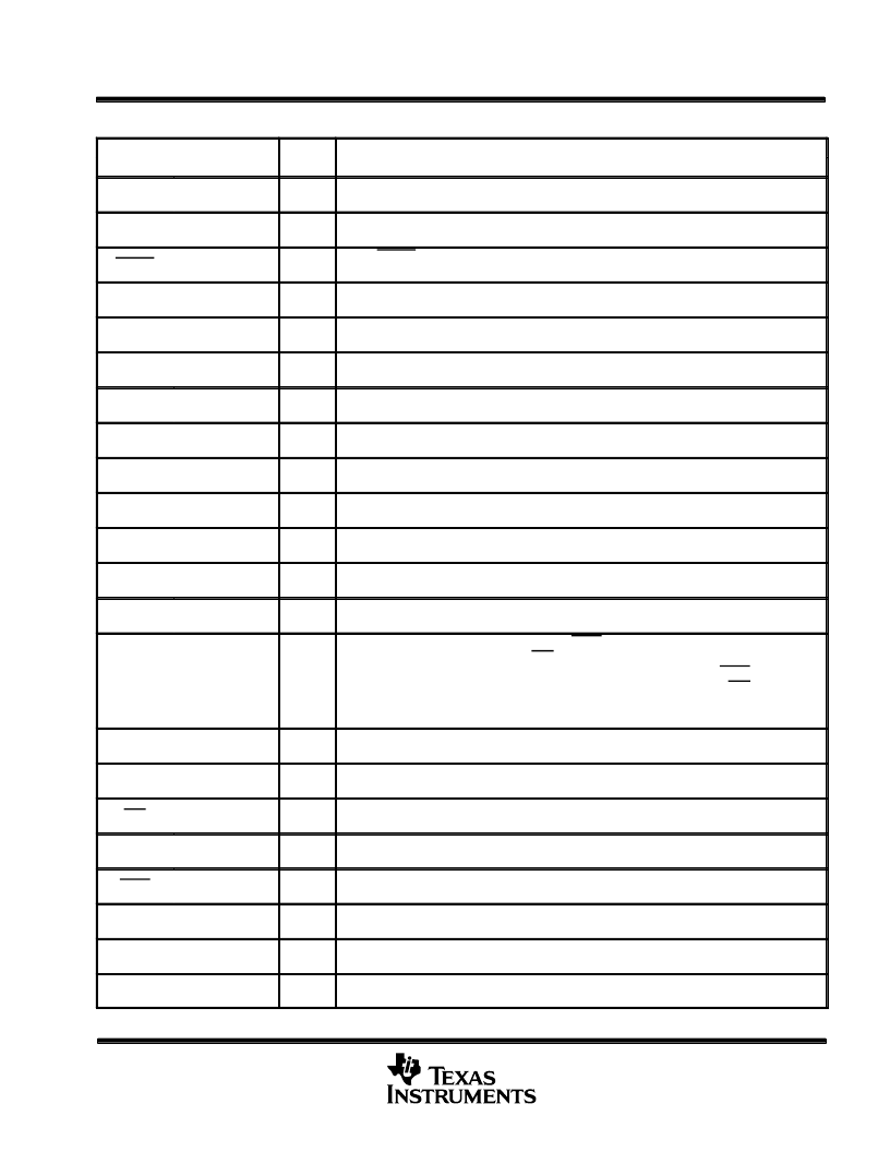
Terminal Functions (continued)
PIN
I/O
TYPE
DESCRIPTION
NAME
NO.
PGND
54, 59, 66, 70,
73, 75, 78, 82
Pseudo-ECL ground (0-V reference)
PVCC
55, 60, 65, 68,
72, 76, 80, 84
Pseudo-ECL supply voltage, 5 V
±
5%
RESET
49
I
(CMOS)
Taking RESET low for 105 ns minimum resets the transmit side of the device. The device must
be reset after power is applied.
RFE
31
O
(CMOS)
Receive framing error. This output goes high whenever a framing error has been detected. The
output is synchronous with the third A2 byte.
RXBC
24
O
(CMOS)
Receive clock. This clock outputs the data from the TDC2302B on the falling edge of the signal.
The clock frequency is either 19.44 MHz (byte clock) or 38.88 MHz (nibble clock).
RXBD(7–0)
22–19, 17–14
O
(CMOS)
Receive data. Terminal-side output data, either byte-or-nibble wide, depending on the state of
the NIB input.
RXF
26
O
(CMOS)
Receive frame. This output provides a positive pulse in synchronization with the third A2 byte
of the SONET/SDH frame.
RXRF
9
O
(TTL)
Receive reference frame. An 8-KHz output derived from the input serial clock RXSC.
RXSCC
83
I
(PECL)
Receive serial clock complement. Used with RXSCT to provide a differential clock input.
RXSCT
81
I
(PECL)
Receive serial clock true. Used with RXSCC to provide a differential clock input that
accompanies the serial data input.
RXSDC
79
I
(PECL)
Receive serial data input complement. Used with RXSDT to provide a differential data input.
RXSDT
77
I
(PECL)
Receive serial data input true. Used with RXSDC to provide a differential data input.
TLB
52
I
(TTL)
Terminal loopback. When this input is high, the terminal input data is looped back to the terminal
output. The terminal input data is also sent to the serial output.
TPINV
10
I
(TTL)
Transmit path invert. When TPINV is low, the TXRF output is active low and clocked out on the
rising edge of TXRC. In addition, the TXF input is active low and clocked into the TDC2302B,
along with TXBDn, on the falling edge of TXBC. When TPINV is high, TXRF becomes an
active-high output that is clocked out on the falling edge of TXRC. Also, TXF becomes an
active-high input that is clocked into the TDC2302B, along with TXBDn, on the rising edge of
TXBC.
TXBC
44
I
(CMOS)
Transmit clock. Terminal-side input clock, either 19.44 MHz (byte data) or 38.88 MHz (nibble
data). The data on TXBDn is clocked into the device on the falling edge of TXBC.
TXBD(7–0)
35–42
I
(CMOS)
Transmit data. Terminal-side input data, either byte or nibble wide.
TXF
50
I
(CMOS)
Transmit frame. This active-low input is synchronous with the third A2 byte of the terminal input
and is required to perform signal scrambling.
TXRC
47
O
(CMOS)
Transmit reference clock. A clock output occurring at the rate of 19.44 MHz or 38.88 MHz,
depending on the state of the NIB input.
TXRF
32
O
(CMOS)
Transmit reference frame. An active-low, one-byte-clock-wide pulse occurring at the frame rate
of 8 kHz.
TXSCC
58
O
(PECL)
Transmit serial clock output complement. Inverter pseudo-ECL clock output.
TXSCT
57
O
(PECL)
Transmit serial clock output true. Noninverted pseudo-ECL clock output.
TXSDC
64
O
(PECL)
Transmit serial data output complement. Inverted pseudo-ECL data output.
相關(guān)PDF資料 |
PDF描述 |
|---|---|
| TEA1721AT | Ultra-low standby SMPS controller with integrated power switch |
| TEC3016 | High-Speed RISC Delay Modules |
| TEC3020 | High-Speed RISC Delay Modules |
| TFB2022AM | Futurebus+ Data Path Unit(面向未來總線數(shù)據(jù)線單元) |
| TFS183B | Development specification |
相關(guān)代理商/技術(shù)參數(shù) |
參數(shù)描述 |
|---|---|
| TDC-24-AKA-030 | 制造商:ATC DIVERSIFIED ELECTRONICS 功能描述:TIME DELAY RELAY DELAY ON OPERATE (RELAY OUTPUT) |
| TDC-24-AKA-060 | 制造商:ATC 功能描述: 制造商:American Technical Ceramics Corp 功能描述: |
| TDC274035NSE-F | 制造商:CDE 制造商全稱:Cornell Dubilier Electronics 功能描述:Dipped, Radial Leaded, Solid Tantalum Capacitors |
| TDC274050NSE-F | 制造商:CDE 制造商全稱:Cornell Dubilier Electronics 功能描述:Dipped, Radial Leaded, Solid Tantalum Capacitors |
| TDC274K035NLE | 制造商:Mallory Sonalert Products Inc 功能描述: |
發(fā)布緊急采購,3分鐘左右您將得到回復(fù)。