- 您現(xiàn)在的位置:買賣IC網(wǎng) > PDF目錄373606 > TC9325F (Toshiba Corporation) Single-Chip DTS Microcontroller (DTS-20) PDF資料下載
參數(shù)資料
| 型號: | TC9325F |
| 廠商: | Toshiba Corporation |
| 英文描述: | Single-Chip DTS Microcontroller (DTS-20) |
| 中文描述: | 單芯片微丘(丘- 20) |
| 文件頁數(shù): | 5/101頁 |
| 文件大?。?/td> | 1802K |
| 代理商: | TC9325F |
第1頁第2頁第3頁第4頁當(dāng)前第5頁第6頁第7頁第8頁第9頁第10頁第11頁第12頁第13頁第14頁第15頁第16頁第17頁第18頁第19頁第20頁第21頁第22頁第23頁第24頁第25頁第26頁第27頁第28頁第29頁第30頁第31頁第32頁第33頁第34頁第35頁第36頁第37頁第38頁第39頁第40頁第41頁第42頁第43頁第44頁第45頁第46頁第47頁第48頁第49頁第50頁第51頁第52頁第53頁第54頁第55頁第56頁第57頁第58頁第59頁第60頁第61頁第62頁第63頁第64頁第65頁第66頁第67頁第68頁第69頁第70頁第71頁第72頁第73頁第74頁第75頁第76頁第77頁第78頁第79頁第80頁第81頁第82頁第83頁第84頁第85頁第86頁第87頁第88頁第89頁第90頁第91頁第92頁第93頁第94頁第95頁第96頁第97頁第98頁第99頁第100頁第101頁
TC9325F
2002-05-14
5
Pin No.
Symbol
Pin Name
Function and Operation
Remarks
46
DCREF
AD converter
reference voltage
input
AD converter reference voltage input
pin. Normally apply V
DD
.
47~50
P2-0
/ADIN1
P2-3
/ADIN4
I/O port 2
/A/D analog voltage
input
51~54
P3-0
/ADIN5
P3-3
/ADIN8
I/O port 3
/A/D analog voltage
input
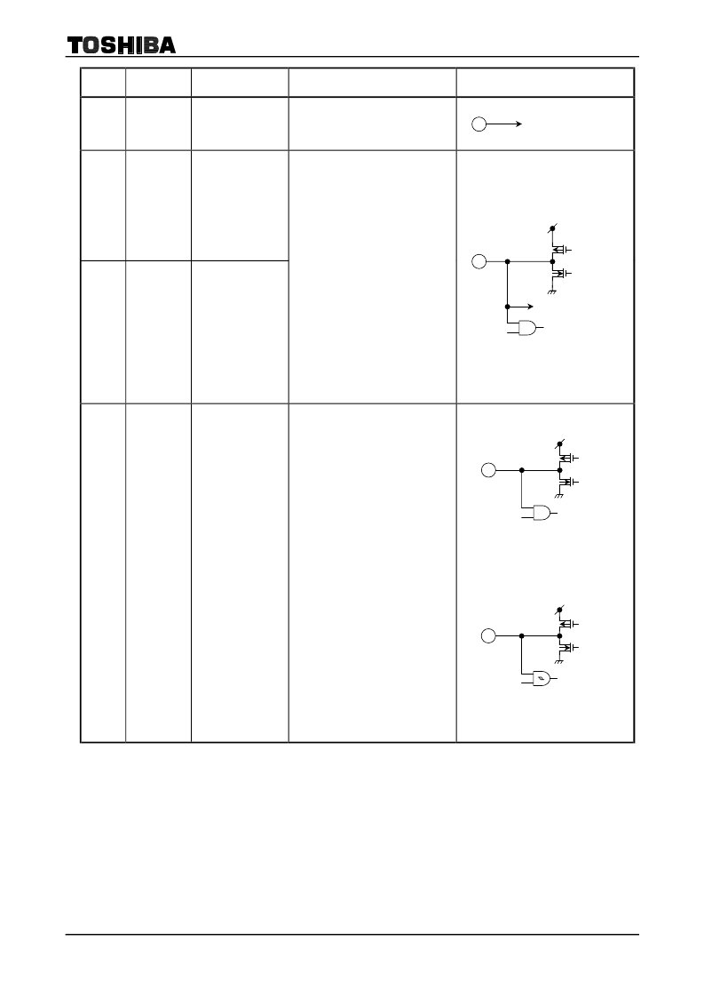
4-bit CMOS I/O ports.
Input and output can be programmed
in 1-bit unit.
Pins P2-0 to P3-3 are also used for
the built-in 8-bit, 8-channel AD
converter analog input.
A built-in AD converter is a
comparison system one by one.
When using a 4.5 MHz oscillator, the
conversion clock can be selected
among 900 kHz, 100 kHz, and 50
kHz. When using a 75 kHz oscillator,
the conversion clock is set to 75 kHz.
The conversion times are respectively
23, 192, 382, and 294
μ
s.
The necessary pins can be
programmed to A/D analog input in
1-bit units. Voltage up to the V
DD
can
be input as the AD converter analog
input voltage.
Settings for the AD converter and its
associated control can be performed
by software.
57
58
59
60
P4-0
P4-1
/SI1
/SI2
P4-2
/SO1
/SO2
P4-3
/SCK1
/SCK2
I/O port 4
Serial data input 1
/Serial data input 2
Serial data
input/output 1
/Serial data input 2
Serial clock
input/output 1
/Serial clock input 2
4-bit CMOS I/O ports.
Input and output can be programmed
in 1-bit unit.
Pins P4-1 to P4-3 also input/output
the two serial interface circuits (SIO1,
SIO2).
On the clock edge of the SCK1 pin,
SIO1 can input 4-bit or 8-bit serial
data to pin SI1 or input/output data to
pin SO1. The clock (SCK1) of serial
operation can perform selection of an
inside (SCK
=
37.5 kHz) /exterior, and
can perform control of various LSI,
and communication between
controllers easily.
Enabling the SIO1 interrupt jumps the
program to address 4 when SIO1
execution completes.
On the falling edge of the SCK2 pin,
SIO2 can input 26-bit serial data to
the SI2 pin.
SIO2 incorporates a data detector.
Enabling the SIO2 interrupt triggers
the interrupt on the falling edge of the
SCK2 pin and jumps the program to
address 6.
The SIO1 and SIO2 inputs all
incorporate Schmitt circuits.
SIO1 and SIO2 and their associated
controls can be used and set by
software.
To AD converter
Input instruction
(P4-0)
V
DD
Input instruction
+
SIOon
(P4-1~P4-3)
V
DD
Input
instruction
V
DD
To AD converter
~
~
相關(guān)PDF資料 |
PDF描述 |
|---|---|
| TC9327 | DTS MICROCONTROLLER |
| TC9327F | DTS MICROCONTROLLER |
| TC9331 | AUDIO DIGITAL SIGNAL PROCESSOR |
| TC9331F | AUDIO DIGITAL SIGNAL PROCESSOR |
| TC9332 | AUDIO DIGITAL SIGNAL PROCESSOR |
相關(guān)代理商/技術(shù)參數(shù) |
參數(shù)描述 |
|---|---|
| TC9327 | 制造商:TOSHIBA 制造商全稱:Toshiba Semiconductor 功能描述:DTS MICROCONTROLLER |
| TC9327BFG | 制造商:TOSHIBA 制造商全稱:Toshiba Semiconductor 功能描述:DTS Microcontroller (DTS-21) |
| TC9327F | 制造商:TOSHIBA 制造商全稱:Toshiba Semiconductor 功能描述:DTS MICROCONTROLLER |
| TC9328AF | 制造商:TOSHIBA 制造商全稱:Toshiba Semiconductor 功能描述:Portable Audio DTS Controller (DTS-21) |
| TC9328AF_04 | 制造商:TOSHIBA 制造商全稱:Toshiba Semiconductor 功能描述:Portable Audio DTS Controller (DTS-21) |
發(fā)布緊急采購,3分鐘左右您將得到回復(fù)。