- 您現(xiàn)在的位置:買賣IC網(wǎng) > PDF目錄361342 > T35L6432A (TM Technology, Inc.) 64K x 32 SRAM PDF資料下載
參數(shù)資料
| 型號: | T35L6432A |
| 廠商: | TM Technology, Inc. |
| 英文描述: | 64K x 32 SRAM |
| 中文描述: | 64K的× 32的SRAM |
| 文件頁數(shù): | 9/15頁 |
| 文件大小: | 1347K |
| 代理商: | T35L6432A |

TE
CH
tm
T35L6432A
Taiwan Memory Technology, Inc. reserves the right
P. 9
to change products or specifications without notice.
Publication Date: DEC. 1998
Revision:A
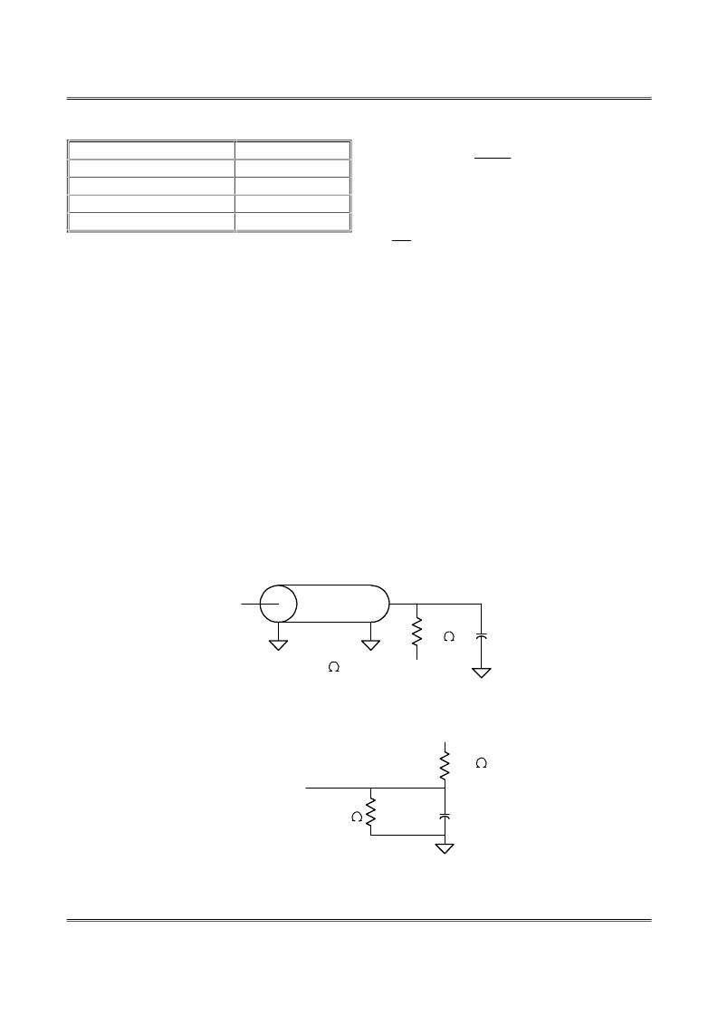
AC TEST CONDITIONS
Input pulse levels
Input rise and fall times
Input timing reference levels
Output reference levels
Output load
Notes:
1. All voltages referenced to VSS (GND).
2. Overshoot:
VIH
≤
+3.6 V for t
≤
tKC/2.
Undershoot: VIL
≤
-1.0 V for t
≤
tKC/2.
3. Icc is given with no output current. Icc increases
with greater output loading and faster cycle
times.
4. This parameter is sampled.
5. Test conditions as specified with the output
loading as shown in Fig. 1 unless otherwise
noted.
6. Output loading is specified with CL = 5 pF as in
Fig. 2.
7. At any given temperature and voltage condition,
tKQHZ is less than tKQLZ and tOEHZ is less
than tOELZ.
0V to 3.0V
1.5ns
1.5V
1.5V
See Figures 1 and 2
8. A READ cycle is defined by byte write enables
all HIGH or
ADSP
LOW along with chip
enables being active for the required setup and
hold times. A WRITE cycle is defined by at one
byte or all byte WRITE per READ/WRITE
TRUTH TABLE.
9.
OE
is a "don't care" when a byte write enable is
sampled LOW.
10.This is a synchronous device. All synchronous
inputs must meet specified setup and hold time,
except for "don't care" as defined in the truth
table.
11.AC I/O curves are available upon request.
12."Device Deselected means the device is in
POWER-DOWN mode as defined in the truth
table. "Device Selected" means the device is
active.
13.Typical values are measured at 3.3V, 25
°
C and
20ns cycle time.
14.MODE pin has an internal pull-up and exhibits
an input leakage current of
±
10
μ
A.
OUTPUT LOADS
DQ
DQ
Fig.1 OUTPUT LOAD EQUIVALENT
Fig.2 OUTPUT LOAD EQUIVALENT
Z
0
= 50
50
30 pF
Vt = 1.5V
3.3V
317
351
5 pF
相關(guān)PDF資料 |
PDF描述 |
|---|---|
| T35L6432A-5Q | 64K x 32 SRAM |
| T35L6432A-5T | 64K x 32 SRAM |
| T35L6432B | 64K x 32 SRAM |
| T35L6432B-10Q | 64K x 32 SRAM |
| T35L6432B-12T | 64K x 32 SRAM |
相關(guān)代理商/技術(shù)參數(shù) |
參數(shù)描述 |
|---|---|
| T35L6432A-5Q | 制造商:TMT 制造商全稱:TMT 功能描述:64K x 32 SRAM |
| T35L6432A-5T | 制造商:TMT 制造商全稱:TMT 功能描述:64K x 32 SRAM |
| T35L6432B | 制造商:TMT 制造商全稱:TMT 功能描述:64K x 32 SRAM |
| T35L6432B-10Q | 制造商:TMT 制造商全稱:TMT 功能描述:64K x 32 SRAM |
| T35L6432B-12T | 制造商:TMT 制造商全稱:TMT 功能描述:64K x 32 SRAM |
發(fā)布緊急采購,3分鐘左右您將得到回復(fù)。