- 您現(xiàn)在的位置:買賣IC網(wǎng) > PDF目錄361342 > T35L6432A (TM Technology, Inc.) 64K x 32 SRAM PDF資料下載
參數(shù)資料
| 型號: | T35L6432A |
| 廠商: | TM Technology, Inc. |
| 英文描述: | 64K x 32 SRAM |
| 中文描述: | 64K的× 32的SRAM |
| 文件頁數(shù): | 12/15頁 |
| 文件大?。?/td> | 1347K |
| 代理商: | T35L6432A |
TE
CH
tm
T35L6432A
Taiwan Memory Technology, Inc. reserves the right
P. 12
to change products or specifications without notice.
Publication Date: DEC. 1998
Revision:A
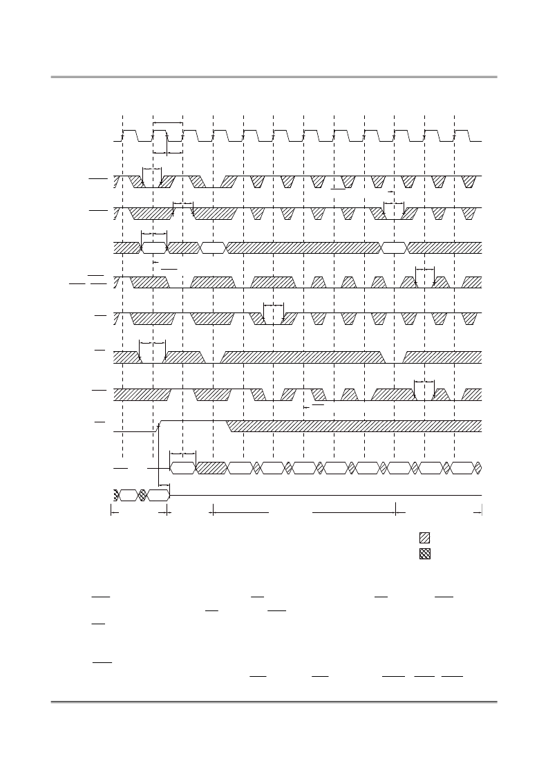
WRITE TIMING
BU RS T W RIT E
C L K
ADS C
Hig h-Z
A DS P
A DDR E S S
B W E ,
B W 1- B W 4
t KC
t KH
t KL
t A DS S
t ADS H
DON'T CARE
UNDEFINED
t AS
t AH
t WS
t WH
t CE S
t CE H
t AAS
t AAH
tO E HZ
t D S
t DH
S ing le W RIT E
(NOT E 3)
D(A1)
D(A2)
D(A2+1 )
D(A2 +2)
D(A2+3 )
D(A3+ 1)
D(A3 )
A3
A 2
A1
(NOT E 1)
C E
( NO T E 2 )
ADV
O E
D
ADS C exte nds bt AD SS
t AD SH
t AD SS
t AD S H
G W
t W S
t WH
D(A2+ 1)
D (A3+2 )
BUR ST RE AD
E xte nde d BU RST W RIT E
Q
AD V suspnds burst .
(NO TE 4)
(N OT E 5)
BY T E W RIT E sig nals a re
ig nored for first cy cle w hen
ADS P init ialte s burst.
Note:
1. Q(A2) refers to output from address A2. Q (A2 + 1) refers to output from the next internal burst
address following A2.
2. CE2 and CE2 have timing identical to CE. On this diagram, when CE is LOW , CE2 is LOW
and CE2 is HIGH. When CE is HIGH , CE2 is HIGH and CE2 is LOW.
3. OE must be HIGH before the input data setup and hold HIGH throughout the data hold time. This
prevents input/output data contention for the time period to the byte write enable inputs being
sampled.
4.
ADV
must be HIGH to permit a WRITE to the loaded address.
5. Full width WRITE can be initiated by GW LOW or GW HIGH and BWE ,BW1-BW4 LOW.
相關(guān)PDF資料 |
PDF描述 |
|---|---|
| T35L6432A-5Q | 64K x 32 SRAM |
| T35L6432A-5T | 64K x 32 SRAM |
| T35L6432B | 64K x 32 SRAM |
| T35L6432B-10Q | 64K x 32 SRAM |
| T35L6432B-12T | 64K x 32 SRAM |
相關(guān)代理商/技術(shù)參數(shù) |
參數(shù)描述 |
|---|---|
| T35L6432A-5Q | 制造商:TMT 制造商全稱:TMT 功能描述:64K x 32 SRAM |
| T35L6432A-5T | 制造商:TMT 制造商全稱:TMT 功能描述:64K x 32 SRAM |
| T35L6432B | 制造商:TMT 制造商全稱:TMT 功能描述:64K x 32 SRAM |
| T35L6432B-10Q | 制造商:TMT 制造商全稱:TMT 功能描述:64K x 32 SRAM |
| T35L6432B-12T | 制造商:TMT 制造商全稱:TMT 功能描述:64K x 32 SRAM |
發(fā)布緊急采購,3分鐘左右您將得到回復(fù)。