- 您現(xiàn)在的位置:買(mǎi)賣IC網(wǎng) > PDF目錄225195 > SM320C50HFGM66 (TEXAS INSTRUMENTS INC) 16-BIT, 66 MHz, OTHER DSP, CQFP132 PDF資料下載
參數(shù)資料
| 型號(hào): | SM320C50HFGM66 |
| 廠商: | TEXAS INSTRUMENTS INC |
| 元件分類: | 數(shù)字信號(hào)處理 |
| 英文描述: | 16-BIT, 66 MHz, OTHER DSP, CQFP132 |
| 封裝: | TIE BAR, CERAMIC, QFP-132 |
| 文件頁(yè)數(shù): | 35/35頁(yè) |
| 文件大小: | 536K |
| 代理商: | SM320C50HFGM66 |
第1頁(yè)第2頁(yè)第3頁(yè)第4頁(yè)第5頁(yè)第6頁(yè)第7頁(yè)第8頁(yè)第9頁(yè)第10頁(yè)第11頁(yè)第12頁(yè)第13頁(yè)第14頁(yè)第15頁(yè)第16頁(yè)第17頁(yè)第18頁(yè)第19頁(yè)第20頁(yè)第21頁(yè)第22頁(yè)第23頁(yè)第24頁(yè)第25頁(yè)第26頁(yè)第27頁(yè)第28頁(yè)第29頁(yè)第30頁(yè)第31頁(yè)第32頁(yè)第33頁(yè)第34頁(yè)當(dāng)前第35頁(yè)
SMJ320C50/SMQ320C50
DIGITAL SIGNAL PROCESSOR
SGUS020 – JUNE 1996
9
POST OFFICE BOX 1443
HOUSTON, TEXAS 77251–1443
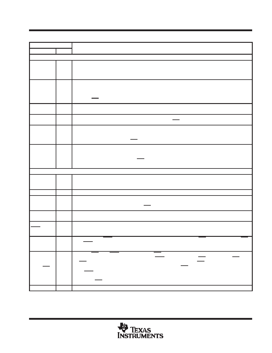
Terminal Functions (continued)
PIN
DESCRIPTION
NAME
TYPE
DESCRIPTION
SERIAL PORT SIGNALS
CLKR
TCLKR
I
Receive clock. External clock signal for clocking data from DR (data receive) or TDR (TDM data receive) into the
RSR (serial port receive shift register). Must be present during serial port transfers. If the serial port is not being used,
these signals can be sampled as an input via the IN0 bit of the serial port control (SPC) or TDR serial port control
(TSPC) registers.
CLKX
TCLKX
I/O/Z
Transmit clock. Clock signal for clocking data from the DR or TDR to the DX (data transmit) or TDX (TDM data
transmit pins). CLKX can be an input if the MCM bit in the serial port control register is set to 0. It can also be driven
by the device at 1/4 the CLKOUT1 frequency when the MCM bit is set to 1. If the serial port is not being used, this
pin can be sampled as an input via the IN1 bit of the SPC or TSPC register. This signal goes into the high-impedance
state when OFF is active (low).
DR
TDR
I
Serial data receive. Serial data is received in the RSR (serial port receive shift register) via DR or TDR.
DX
TDX
O/Z
Serial port transmit. Serial data transmitted from XSR (serial port transmit shift register) via DX or TDX. This signal
is in the high-impedance state when not transmitting and when OFF is active (low).
FSR
TFSR / TADD
I
I/O/Z
Frame synchronization pulse for receive. The falling edge of FSR or TFSR initiates the data receive process, which
begins the clocking of the RSR. TFSR becomes an input / output (TADD) pin when the serial port is operating in the
TDM mode (TDM bit = 1). In TDM mode, this pin is used to input /output the address of the port. This signal goes
into the high-impedance state when OFF is active (low).
FSX
TFSX / TFRM
I/O/Z
Frame synchronization pulse for transmit. The falling edge of FSX/TFSX initiates the data transmit process, which
begins the clocking of the XSR. Following reset, the default operating condition of FSX/TFSX is an input. This pin
may be selected by software to be an output when the TXM bit in the serial control register is set to 1. This signal
goes to the high-impedance state when OFF is active (low). When operating in TDM mode (TDM bit = 1), TFSX
becomes TFRM, the TDM frame-synchronization pulse.
TEST SIGNALS
TCK
I
Boundary scan test clock. This is normally a free-running clock with a 50% duty cycle. The changes of TAP (test
access port) input signals (TMS and TDI) are clocked into the TAP controller, instruction register, or selected test
data register on the rising edge of TCK. Changes at the TAP output signal (TDO) occur on the falling edge of TCK.
TDI
I
Boundary scan test data input. TDI is clocked into the selected register (instruction or data) on a rising edge of TCK.
TDO
O/Z
Boundary scan test data output. The contents of the selected register (instruction or data) is shifted out of TDO on
the falling edge of TCK. TDO is in the high-impedance state except when scanning of data is in progress. This signal
also goes to the high-impedance state when OFF is active (low).
TMS
I
Boundary scan test mode select. This serial control input is clocked into the test access port (TAP) controller on the
rising edge of TCK.
TRST
I
Boundary scan test reset. Asserting this signal gives the JTAG scan system control of the operations of the device.
If this signal is not connected or is driven low, the device operates in its functional mode and the boundary scan
signals are ignored.
EMU0
I/O/Z
Emulator 0. When TRST is driven low, EMU0 must be high for activation of the OFF condition (see EMU1/OFF).
When TRST is driven high, EMU0 is used as an interrupt to or from the emulator system and is defined as input/output
put via boundary scan.
EMU1 / OFF
I/O/Z
Emulator 1/OFF. When TRST is driven high, EMU1 / OFF is used as an interrupt to or from the emulator system and
is defined as input/output via boundary scan. When TRST is driven low, EMU1 / OFF is configured as OFF. When
the OFF signal is active (low), all output drivers are in the high-impedance state. OFF is used exclusively for testing
and emulation purposes (not for multiprocessing applications). For the OFF condition, the following conditions apply:
TRST = Low
EMU0 = High
EMU1/OFF = Low
RESERVED
N/C
Reserved. This pin must be left unconnected.
I = input, O = output, Z = high-impedance
Quad flat pack only
相關(guān)PDF資料 |
PDF描述 |
|---|---|
| SM5272B-2 | 3 RF DECODER |
| SM5272B-3 | 3 RF DECODER |
| SM5272B-4 | 3 RF DECODER |
| SM5272B-5 | 3 RF DECODER |
| SM5272B-6 | 3 RF DECODER |
相關(guān)代理商/技術(shù)參數(shù) |
參數(shù)描述 |
|---|---|
| SM320C50PQI80EP | 功能描述:數(shù)字信號(hào)處理器和控制器 - DSP, DSC EP Digital Signal Proc RoHS:否 制造商:Microchip Technology 核心:dsPIC 數(shù)據(jù)總線寬度:16 bit 程序存儲(chǔ)器大小:16 KB 數(shù)據(jù) RAM 大小:2 KB 最大時(shí)鐘頻率:40 MHz 可編程輸入/輸出端數(shù)量:35 定時(shí)器數(shù)量:3 設(shè)備每秒兆指令數(shù):50 MIPs 工作電源電壓:3.3 V 最大工作溫度:+ 85 C 封裝 / 箱體:TQFP-44 安裝風(fēng)格:SMD/SMT |
| SM320C50PQM66EP | 功能描述:數(shù)字信號(hào)處理器和控制器 - DSP, DSC EP Digital Signal Proc RoHS:否 制造商:Microchip Technology 核心:dsPIC 數(shù)據(jù)總線寬度:16 bit 程序存儲(chǔ)器大小:16 KB 數(shù)據(jù) RAM 大小:2 KB 最大時(shí)鐘頻率:40 MHz 可編程輸入/輸出端數(shù)量:35 定時(shí)器數(shù)量:3 設(shè)備每秒兆指令數(shù):50 MIPs 工作電源電壓:3.3 V 最大工作溫度:+ 85 C 封裝 / 箱體:TQFP-44 安裝風(fēng)格:SMD/SMT |
| SM320C6000GDP167 | 制造商:TI 制造商全稱:Texas Instruments 功能描述:FLOATING-POINT DIGITAL SIGNAL PROCESSOR |
| SM320C6000GDP200 | 制造商:TI 制造商全稱:Texas Instruments 功能描述:FLOATING-POINT DIGITAL SIGNAL PROCESSOR |
| SM320C6000GDP225 | 制造商:TI 制造商全稱:Texas Instruments 功能描述:FLOATING-POINT DIGITAL SIGNAL PROCESSOR |
發(fā)布緊急采購(gòu),3分鐘左右您將得到回復(fù)。