- 您現(xiàn)在的位置:買賣IC網(wǎng) > PDF目錄225195 > SM320C50HFGM66 (TEXAS INSTRUMENTS INC) 16-BIT, 66 MHz, OTHER DSP, CQFP132 PDF資料下載
參數(shù)資料
| 型號(hào): | SM320C50HFGM66 |
| 廠商: | TEXAS INSTRUMENTS INC |
| 元件分類: | 數(shù)字信號(hào)處理 |
| 英文描述: | 16-BIT, 66 MHz, OTHER DSP, CQFP132 |
| 封裝: | TIE BAR, CERAMIC, QFP-132 |
| 文件頁數(shù): | 2/35頁 |
| 文件大?。?/td> | 536K |
| 代理商: | SM320C50HFGM66 |
第1頁當(dāng)前第2頁第3頁第4頁第5頁第6頁第7頁第8頁第9頁第10頁第11頁第12頁第13頁第14頁第15頁第16頁第17頁第18頁第19頁第20頁第21頁第22頁第23頁第24頁第25頁第26頁第27頁第28頁第29頁第30頁第31頁第32頁第33頁第34頁第35頁
SMJ320C50/SMQ320C50
DIGITAL SIGNAL PROCESSOR
SGUS020 – JUNE 1996
10
POST OFFICE BOX 1443
HOUSTON, TEXAS 77251–1443
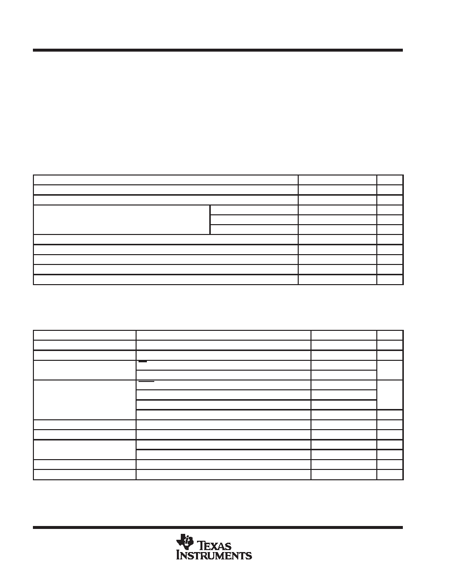
absolute maximum ratings over operating free-air temperature range (unless otherwise noted)
Supply voltage range, VDD (see Note 1)
– 0.3 V to 7 V
. . . . . . . . . . . . . . . . . . . . . . . . . . . . . . . . . . . . . . . . . . . . .
Input voltage range
– 0.3 V to 7 V
. . . . . . . . . . . . . . . . . . . . . . . . . . . . . . . . . . . . . . . . . . . . . . . . . . . . . . . . . . . . . . .
Output voltage range
– 0.3 V to 7 V
. . . . . . . . . . . . . . . . . . . . . . . . . . . . . . . . . . . . . . . . . . . . . . . . . . . . . . . . . . . . . .
Maximum operating case temperature, TC
125
°C
. . . . . . . . . . . . . . . . . . . . . . . . . . . . . . . . . . . . . . . . . . . . . . . . . .
Minimum operating free-air temperature, TA
– 55
°C
. . . . . . . . . . . . . . . . . . . . . . . . . . . . . . . . . . . . . . . . . . . . . . . .
Storage temperature range, Tstg
– 65
°C to 150°C
. . . . . . . . . . . . . . . . . . . . . . . . . . . . . . . . . . . . . . . . . . . . . . . . . .
Stresses beyond those listed under “absolute maximum ratings” may cause permanent damage to the device. These are stress ratings only and
functional operation of the device at these or any other conditions beyond those indicated under “recommended operating conditions” is not
implied. Exposure to absolute-maximum-rated conditions for extended periods may affect device reliability.
NOTE 1: All voltage values are with respect to VSS.
recommended operating conditions
MIN
NOM
MAX
UNIT
VDD
Supply voltage
4.75
5
5.25
V
VSS
Supply voltage
0
V
CLKIN, CLKIN2
3.0
VDD + 0.3
V
VIH
High-level input voltage
CLKX, CLKR, TCLKX, TCLKR
2.5
VDD + 0.3
V
All others
2.2
VDD + 0.3
V
VIL
Low-level input voltage
– 0.3
0.6
V
IOH
High-level output current
– 300
A
IOL
Low-level output current
2
mA
TC
Operating case temperature
125
°C
TA
Operating free-air temperature
– 55
°C
This IOH can be exceeded when using a 1-K pulldown resistor on the TDM serial port TADD output, however this output still meets VOH
specifications under these conditions.
electrical characteristics over recommended ranges of supply voltage and operating free-air
temperature (unless otherwise noted)
PARAMETER
TEST CONDITIONS§
MIN
TYP
MAX
UNIT
VOH
High-level output voltage#
IOH = MAX
2.4
3
V
VOL
Low-level output voltage
IOL = MAX
0.3
0.6
V
IOZ
High-impedance output
BR (with internal pullup)
– 500
||
30
A
IOZ
g
current (VDD = MAX)
All others
– 30
||
30
A
TRST (with internal pulldown)
– 30
||
800
II
Input current
TMS, TCK, TDI (with internal pullups)
– 500
||
30
A
II
(VI = VSS to VDD)
X2/CLKIN
– 50
||
50
All other inputs
– 30
||
30
A
IDDC
Supply current, core CPU
Operating,
TA = 25°C,
VDD = 5.25 V, fx = 50 MHz
60
225
mA
IDDP
Supply current, pins
Operating,
TA = 25°C,
VDD = 5.25 V, fx = 50 MHz
40
225
mA
IDD
Supply current standby
IDLE instruction,
TA = 125°C,
VDD = 5.25 V, fx = 50 MHz
30
mA
IDD
Supply current, standby
IDLE2 instruction, Clocks shut off, TA =125°C,
VDD =5.25 V
7
A
Ci
Input capacitance
15
40
pF
Co
Output capacitance
15
40
pF
§ For conditions shown as MIN / MAX, use the appropriate value specified under recommended operating conditions.
All typical or nominal values are at VDD = 5 V, TA = 25°C.
# All input and output voltage levels are TTL-compatible. Figure 1 shows the test load circuit; Figure 2 and Figure 3 show the voltage reference
levels.
|| These values are not specified pending detailed characterization.
相關(guān)PDF資料 |
PDF描述 |
|---|---|
| SM5272B-2 | 3 RF DECODER |
| SM5272B-3 | 3 RF DECODER |
| SM5272B-4 | 3 RF DECODER |
| SM5272B-5 | 3 RF DECODER |
| SM5272B-6 | 3 RF DECODER |
相關(guān)代理商/技術(shù)參數(shù) |
參數(shù)描述 |
|---|---|
| SM320C50PQI80EP | 功能描述:數(shù)字信號(hào)處理器和控制器 - DSP, DSC EP Digital Signal Proc RoHS:否 制造商:Microchip Technology 核心:dsPIC 數(shù)據(jù)總線寬度:16 bit 程序存儲(chǔ)器大小:16 KB 數(shù)據(jù) RAM 大小:2 KB 最大時(shí)鐘頻率:40 MHz 可編程輸入/輸出端數(shù)量:35 定時(shí)器數(shù)量:3 設(shè)備每秒兆指令數(shù):50 MIPs 工作電源電壓:3.3 V 最大工作溫度:+ 85 C 封裝 / 箱體:TQFP-44 安裝風(fēng)格:SMD/SMT |
| SM320C50PQM66EP | 功能描述:數(shù)字信號(hào)處理器和控制器 - DSP, DSC EP Digital Signal Proc RoHS:否 制造商:Microchip Technology 核心:dsPIC 數(shù)據(jù)總線寬度:16 bit 程序存儲(chǔ)器大小:16 KB 數(shù)據(jù) RAM 大小:2 KB 最大時(shí)鐘頻率:40 MHz 可編程輸入/輸出端數(shù)量:35 定時(shí)器數(shù)量:3 設(shè)備每秒兆指令數(shù):50 MIPs 工作電源電壓:3.3 V 最大工作溫度:+ 85 C 封裝 / 箱體:TQFP-44 安裝風(fēng)格:SMD/SMT |
| SM320C6000GDP167 | 制造商:TI 制造商全稱:Texas Instruments 功能描述:FLOATING-POINT DIGITAL SIGNAL PROCESSOR |
| SM320C6000GDP200 | 制造商:TI 制造商全稱:Texas Instruments 功能描述:FLOATING-POINT DIGITAL SIGNAL PROCESSOR |
| SM320C6000GDP225 | 制造商:TI 制造商全稱:Texas Instruments 功能描述:FLOATING-POINT DIGITAL SIGNAL PROCESSOR |
發(fā)布緊急采購,3分鐘左右您將得到回復(fù)。