- 您現(xiàn)在的位置:買賣IC網(wǎng) > PDF目錄368618 > SI7116DN (Vishay Intertechnology,Inc.) N-Channel 40-V (D-S) Fast Switching MOSFET PDF資料下載
參數(shù)資料
| 型號: | SI7116DN |
| 廠商: | Vishay Intertechnology,Inc. |
| 英文描述: | N-Channel 40-V (D-S) Fast Switching MOSFET |
| 中文描述: | N通道40 - V(下局副局長)快速開關(guān)MOSFET |
| 文件頁數(shù): | 2/5頁 |
| 文件大小: | 78K |
| 代理商: | SI7116DN |
Si7116DN
Vishay Siliconix
www.vishay.com
2
Document Number: 73139
S-51412—Rev. C, 01-Aug-05
Parameter
Symbol
Test Condition
Min
Typ
Max
Unit
Static
Gate Threshold Voltage
V
GS(th)
V
DS
= V
GS
, I
D
= 250 A
1.5
2.5
V
Gate-Body Leakage
I
GSS
V
DS
= 0 V, V
GS
=
20 V
100
nA
Zero Gate Voltage Drain Current
I
DSS
V
DS
= 40 V, V
GS
= 0 V
1
A
V
DS
= 40 V, V
GS
= 0 V, T
J
= 55 C
5
On-State Drain Current
a
I
D(on)
V
DS
5 V, V
GS
= 10
V
40
A
Drain-Source On-State Resistance
a
r
DS(on)
V
GS
= 10
V, I
D
= 16.4 A
0.0065
0.0078
V
GS
= 4.5 V, I
D
= 14.5 A
0.0083
0.010
Forward Transconductance
a
g
fs
V
DS
= 15 V, I
D
= 16.4 A
68
S
Diode Forward Voltage
a
V
SD
I
S
= 3.2 A, V
GS
= 0 V
0.8
1.2
V
Dynamic
b
Total Gate Charge
Q
g
Q
gs
Q
gd
15
23
Gate-Source Charge
= 20 V,
= 4.5 V, I
= 16.4 A
V
DS
V
GS
4.5 V, I
D
16.4 A
6.7
nC
Gate-Drain Charge
5.1
Gate-Resistance
R
g
f = 1 MHz
0.7
1.4
2.1
Turn-On Delay Time
t
d(on)
10
15
Rise Time
t
r
V
= 20 V, R
= 20
1 A, V
GEN
= 10 V, R
g
= 6
10
15
Turn-Off Delay Time
t
d(off)
I
D
36
55
ns
Fall Time
t
f
10
15
Source-Drain Reverse Recovery Time
t
rr
I
F
= 3.2 A, di/dt = 100 A/ s
30
60
Body Diode Reverse Recovery Charge
Q
rr
I
F
= 3.2 A, di/dt = 100 A/ s
26
52
nc
Notes
a.
b.
Stresses beyond those listed under “Absolute Maximum Ratings” may cause permanent damage to the device. These are stress ratings only, and functional operation
of the device at these or any other conditions beyond those indicated in the operational sections of the specifications is not implied. Exposure to absolute maximum rating
conditions for extended periods may affect device reliability.
Pulse test; pulse width
300 s, duty cycle
2%.
Guaranteed by design, not subject to production testing.
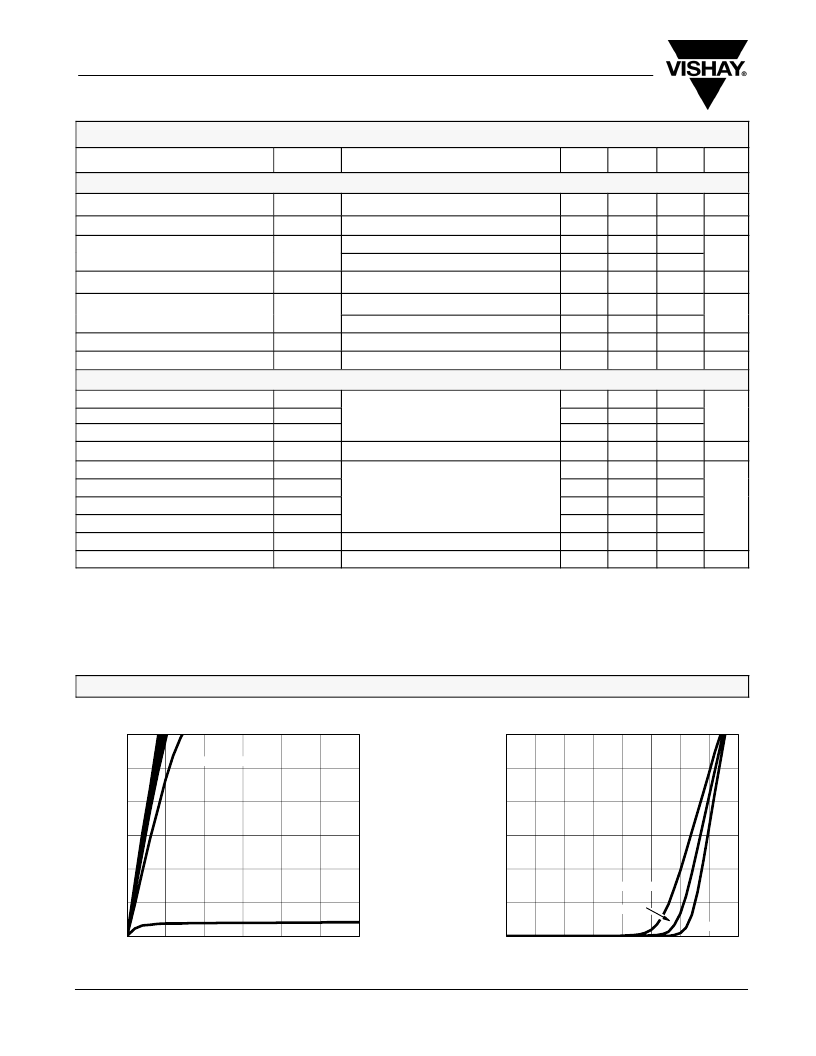
0
10
20
30
40
50
60
0.0
0.5
1.0
1.5
2.0
2.5
3.0
3.5
4.0
0
10
20
30
40
50
60
0.0
0.5
1.0
1.5
2.0
2.5
3.0
V
GS
= 10 thru 4 V
25 C
T
C
= 125 C
–55 C
3 V
Output Characteristics
Transfer Characteristics
V
DS
– Drain-to-Source Voltage (V)
–
I
D
V
GS
– Gate-to-Source Voltage (V)
–
I
D
相關(guān)PDF資料 |
PDF描述 |
|---|---|
| SI7212DN | Dual N-Channel 30-V (D-S) MOSFET with Schottky Diode |
| Si7212DN-T1-E3 | Dual N-Channel 30-V (D-S) MOSFET with Schottky Diode |
| SI7214DN | Dual N-Channel 30-V (D-S) MOSFET with Schottky Diode |
| SI7348DP | N-Channel 20-V (D-S) MOSFET |
| SI7403BDN | P-Channel 20-V (D-S) MOSFET, Low-Threshold |
相關(guān)代理商/技術(shù)參數(shù) |
參數(shù)描述 |
|---|---|
| SI7116DN-T1-E3 | 功能描述:MOSFET 40V 16.4A 3.8W 7.8mohm @ 10V RoHS:否 制造商:STMicroelectronics 晶體管極性:N-Channel 汲極/源極擊穿電壓:650 V 閘/源擊穿電壓:25 V 漏極連續(xù)電流:130 A 電阻汲極/源極 RDS(導(dǎo)通):0.014 Ohms 配置:Single 最大工作溫度: 安裝風(fēng)格:Through Hole 封裝 / 箱體:Max247 封裝:Tube |
| SI7116DN-T1-GE3 | 功能描述:MOSFET 40V 16.4A 3.8W 7.8mohm @ 10V RoHS:否 制造商:STMicroelectronics 晶體管極性:N-Channel 汲極/源極擊穿電壓:650 V 閘/源擊穿電壓:25 V 漏極連續(xù)電流:130 A 電阻汲極/源極 RDS(導(dǎo)通):0.014 Ohms 配置:Single 最大工作溫度: 安裝風(fēng)格:Through Hole 封裝 / 箱體:Max247 封裝:Tube |
| SI7117DNT1E3 | 制造商:VISHAY 功能描述:Pb Free |
| SI7117DN-T1-E3 | 功能描述:MOSFET 150V 2.17A 12.5W 1.2ohm @ 10V RoHS:否 制造商:STMicroelectronics 晶體管極性:N-Channel 汲極/源極擊穿電壓:650 V 閘/源擊穿電壓:25 V 漏極連續(xù)電流:130 A 電阻汲極/源極 RDS(導(dǎo)通):0.014 Ohms 配置:Single 最大工作溫度: 安裝風(fēng)格:Through Hole 封裝 / 箱體:Max247 封裝:Tube |
| SI7117DN-T1-GE3 | 功能描述:MOSFET 150V 2.17A 12.5W 1.2ohm @ 10V RoHS:否 制造商:STMicroelectronics 晶體管極性:N-Channel 汲極/源極擊穿電壓:650 V 閘/源擊穿電壓:25 V 漏極連續(xù)電流:130 A 電阻汲極/源極 RDS(導(dǎo)通):0.014 Ohms 配置:Single 最大工作溫度: 安裝風(fēng)格:Through Hole 封裝 / 箱體:Max247 封裝:Tube |
發(fā)布緊急采購,3分鐘左右您將得到回復(fù)。