- 您現(xiàn)在的位置:買賣IC網(wǎng) > PDF目錄230911 > R5F363A6NFA 16-BIT, FLASH, 20 MHz, MICROCONTROLLER, PQFP100 PDF資料下載
參數(shù)資料
| 型號: | R5F363A6NFA |
| 元件分類: | 微控制器/微處理器 |
| 英文描述: | 16-BIT, FLASH, 20 MHz, MICROCONTROLLER, PQFP100 |
| 封裝: | 14 X 20 MM, 0.65 MM PITCH, PLASTIC, QFP-100 |
| 文件頁數(shù): | 67/115頁 |
| 文件大小: | 2363K |
| 代理商: | R5F363A6NFA |
第1頁第2頁第3頁第4頁第5頁第6頁第7頁第8頁第9頁第10頁第11頁第12頁第13頁第14頁第15頁第16頁第17頁第18頁第19頁第20頁第21頁第22頁第23頁第24頁第25頁第26頁第27頁第28頁第29頁第30頁第31頁第32頁第33頁第34頁第35頁第36頁第37頁第38頁第39頁第40頁第41頁第42頁第43頁第44頁第45頁第46頁第47頁第48頁第49頁第50頁第51頁第52頁第53頁第54頁第55頁第56頁第57頁第58頁第59頁第60頁第61頁第62頁第63頁第64頁第65頁第66頁當(dāng)前第67頁第68頁第69頁第70頁第71頁第72頁第73頁第74頁第75頁第76頁第77頁第78頁第79頁第80頁第81頁第82頁第83頁第84頁第85頁第86頁第87頁第88頁第89頁第90頁第91頁第92頁第93頁第94頁第95頁第96頁第97頁第98頁第99頁第100頁第101頁第102頁第103頁第104頁第105頁第106頁第107頁第108頁第109頁第110頁第111頁第112頁第113頁第114頁第115頁
REJ03B0271-0100 Rev.1.00 Sep 15, 2009
Page 55 of 113
M16C/63 Group
5. Electrical Characteristics
5.1.5
Flash Memory Electrical Characteristics
Notes:
1.
Set the PM17 bit in the PM1 register to 1 (one wait).
2.
When the frequency is 1.8
≤ V
CC1 ≤ 3.0 V, set the FMR17 bit in the FMR1 register to 0 (one wait) or the PM17 bit
in the PM1 register to 1 (one wait)
Notes:
1.
Definition of program and erase cycles:
The program and erase cycles refer to the number of per-block erasures. If the program and erase cycles are n
(n = 1,000), each block can be erased n times. For example, if a 64 Kbyte block is erased after writing two word
data 16,384 times, each to a different address, this counts as one program and erase cycles. Data cannot be
written to the same address more than once without erasing the block (rewrite prohibited).
2.
Cycles to guarantee all electrical characteristics after program and erase. (1 to Min. value can be guaranteed).
3.
In a system that executes multiple programming operations, the actual erasure count can be reduced by writing
to sequential addresses in turn so that as much of the block as possible is used up before performing an erase
operation. It is advisable to retain data on the erasure cycles of each block and limit the number of erase
operations to a certain number.
4.
If an error occurs during block erase, attempt to execute the clear status register command, then execute the
block erase command at least three times until the erase error does not occur.
5.
Customers desiring program/erase failure rate information should contact their Renesas technical support
representative.
6.
The data hold time includes time that the power supply is off or the clock is not supplied.
7.
After an erase start or erase restart, if an interval of at least 20 ms is not set before the next suspend request, the
erase sequence cannot be completed.
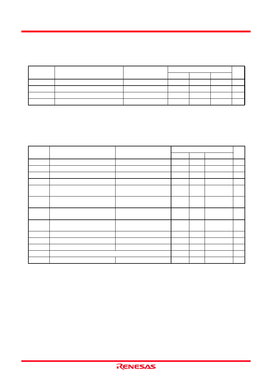
Table 5.9
CPU Clock When Operating Flash Memory (f(BCLK))
VCC1 = 1.8 to 5.5 V, Topr = -20 to 85°C/-40 to 85°C unless otherwise specified.
Symbol
Parameter
Conditions
Standard
Unit
Min.
Typ.
Max.
-
CPU rewrite mode
10 (1)
MHz
f(SLOW_R)
Slow read mode
5MHz
-
Low current consumption read mode
fC(32.768)
35
kHz
-
Data flash read
3.0 V < VCC1 ≤ 5.5 V
20 (2)
MHz
Table 5.10
Flash Memory (Program ROM 1, 2) Electrical Characteristics
VCC1 = 2.7 to 5.5 V at Topr = 0 to 60°C (option: -40°C to 85°C), unless otherwise specified.
Symbol
Parameter
Conditions
Standard
Unit
Min.
Typ.
Max.
-
1,000 (2)
times
-
Two words program time
VCC1 = 3.3 V, Topr = 25°C
150
4000
μs
-
Lock bit program time
VCC1 = 3.3 V, Topr = 25°C
70
3000
μs
-
Block erase time
VCC1 = 3.3 V, Topr = 25°C
0.2
3.0
s
td(SR-SUS)
Time delay from suspend request
until suspend
5 + CPU clock
× 3 cycles
ms
-
Interval from erase start/restart
until following suspend request
0
μs
-
Suspend interval necessary for
auto-erasure to complete (7)
20
ms
-
Time from suspend until erase
restart
30 + CPU
clock × 1 cycle
μs
-
Program, erase voltage
2.7
5.5
V
-
Read voltage
2.7
5.5
V
-
Program, erase temperature
0
60
°C
tPS
Flash Memory Circuit Stabilization Wait Time
50
μs
-
Data hold time (6)
Ambient temperature = 55
°C
20
year
相關(guān)PDF資料 |
PDF描述 |
|---|---|
| R5F363A6NFB | 16-BIT, FLASH, 20 MHz, MICROCONTROLLER, PQFP100 |
| RTC-6583 | REAL TIME CLOCK, PDSO24 |
| R5F61644N50FPV | 32-BIT, FLASH, 50 MHz, MICROCONTROLLER, PQFP144 |
| R5F3650EDFA | MICROCONTROLLER, PQFP100 |
| R5F3650EDFB | MICROCONTROLLER, PQFP100 |
相關(guān)代理商/技術(shù)參數(shù) |
參數(shù)描述 |
|---|---|
| R5F363A6NFA_11 | 制造商:RENESAS 制造商全稱:Renesas Technology Corp 功能描述:This MCU consumes low power, and supports operating modes |
| R5F363A6NFB | 制造商:Renesas Electronics Corporation 功能描述: |
| R5F363A6NFB#U0 | 制造商:Renesas Electronics Corporation 功能描述: |
| R5F363A6NLG | 制造商:RENESAS 制造商全稱:Renesas Technology Corp 功能描述:This MCU consumes low power, and supports operating modes |
| R5F363AEDFA | 制造商:RENESAS 制造商全稱:Renesas Technology Corp 功能描述:RENESAS MCU |
發(fā)布緊急采購,3分鐘左右您將得到回復(fù)。