- 您現(xiàn)在的位置:買賣IC網(wǎng) > PDF目錄230911 > R5F363A6NFA 16-BIT, FLASH, 20 MHz, MICROCONTROLLER, PQFP100 PDF資料下載
參數(shù)資料
| 型號(hào): | R5F363A6NFA |
| 元件分類: | 微控制器/微處理器 |
| 英文描述: | 16-BIT, FLASH, 20 MHz, MICROCONTROLLER, PQFP100 |
| 封裝: | 14 X 20 MM, 0.65 MM PITCH, PLASTIC, QFP-100 |
| 文件頁(yè)數(shù): | 27/115頁(yè) |
| 文件大?。?/td> | 2363K |
| 代理商: | R5F363A6NFA |
第1頁(yè)第2頁(yè)第3頁(yè)第4頁(yè)第5頁(yè)第6頁(yè)第7頁(yè)第8頁(yè)第9頁(yè)第10頁(yè)第11頁(yè)第12頁(yè)第13頁(yè)第14頁(yè)第15頁(yè)第16頁(yè)第17頁(yè)第18頁(yè)第19頁(yè)第20頁(yè)第21頁(yè)第22頁(yè)第23頁(yè)第24頁(yè)第25頁(yè)第26頁(yè)當(dāng)前第27頁(yè)第28頁(yè)第29頁(yè)第30頁(yè)第31頁(yè)第32頁(yè)第33頁(yè)第34頁(yè)第35頁(yè)第36頁(yè)第37頁(yè)第38頁(yè)第39頁(yè)第40頁(yè)第41頁(yè)第42頁(yè)第43頁(yè)第44頁(yè)第45頁(yè)第46頁(yè)第47頁(yè)第48頁(yè)第49頁(yè)第50頁(yè)第51頁(yè)第52頁(yè)第53頁(yè)第54頁(yè)第55頁(yè)第56頁(yè)第57頁(yè)第58頁(yè)第59頁(yè)第60頁(yè)第61頁(yè)第62頁(yè)第63頁(yè)第64頁(yè)第65頁(yè)第66頁(yè)第67頁(yè)第68頁(yè)第69頁(yè)第70頁(yè)第71頁(yè)第72頁(yè)第73頁(yè)第74頁(yè)第75頁(yè)第76頁(yè)第77頁(yè)第78頁(yè)第79頁(yè)第80頁(yè)第81頁(yè)第82頁(yè)第83頁(yè)第84頁(yè)第85頁(yè)第86頁(yè)第87頁(yè)第88頁(yè)第89頁(yè)第90頁(yè)第91頁(yè)第92頁(yè)第93頁(yè)第94頁(yè)第95頁(yè)第96頁(yè)第97頁(yè)第98頁(yè)第99頁(yè)第100頁(yè)第101頁(yè)第102頁(yè)第103頁(yè)第104頁(yè)第105頁(yè)第106頁(yè)第107頁(yè)第108頁(yè)第109頁(yè)第110頁(yè)第111頁(yè)第112頁(yè)第113頁(yè)第114頁(yè)第115頁(yè)
REJ03B0271-0100 Rev.1.00 Sep 15, 2009
Page 19 of 113
M16C/63 Group
1. Overview
Notes:
1.
Contact the oscillator manufacturer regarding the oscillation characteristics.
2.
TXD2, SDA2, and SCL2 are N-channel open drain output pins. TXDi, SDAi, and SCLi can be selected as CMOS
output pins or N-channel open drain output pins (i = 0, 1, 5 to 7).
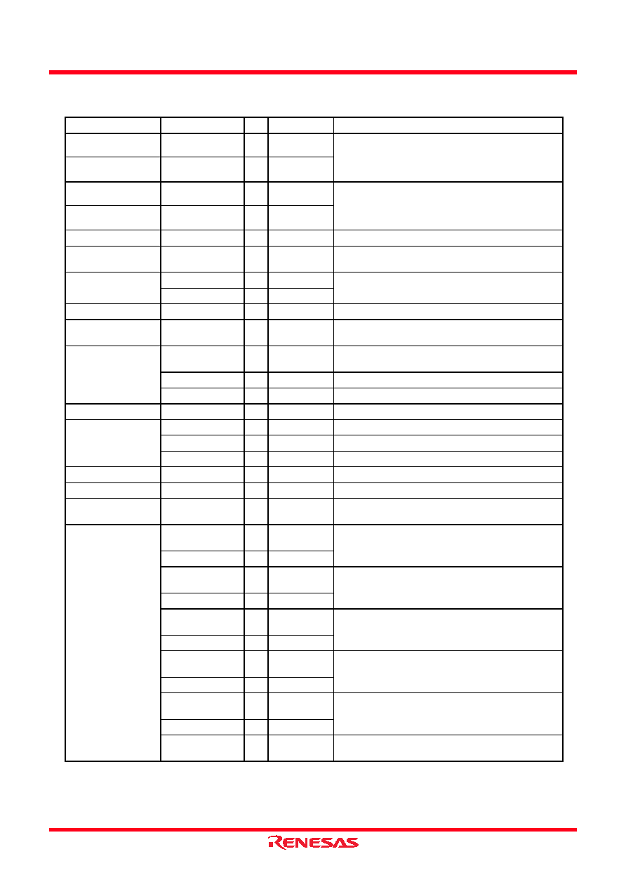
Table 1.11
Pin Functions for the 100-Pin Package (2/3)
Signal Name
Pin Name
I/O
Power Supply
Description
Main clock input
XIN
I
VCC1
I/O for the main clock oscillator. Connect a ceramic
resonator or crystal between pins XIN and XOUT. (1)
Input an external clock to XIN pin and leave XOUT pin
open.
Main clock output
XOUT
O
VCC1
Sub clock input
XCIN
I
VCC1
I/O for a sub clock oscillator. Connect a crystal
between XCIN pin and XCOUT pin. (1) Input an
external clock to XCIN pin and leave XCOUT pin
open.
Sub clock output
XCOUT
O
VCC1
BCLK output
BCLK
O
VCC2
Outputs the BCLK signal.
Clock output
CLKOUT
O
VCC2
Outputs a clock with the same frequency as fC, f1, f8,
or f32.
INT interrupt input
INT0 to INT2
I
VCC1
Input for the
INT interrupt.
INT3 to INT7
I
VCC2
NMI interrupt input
NMI
I
VCC1
Input for the
NMI interrupt.
Key input interrupt
input
KI0 to KI7
I
VCC1
Input for the key input interrupt.
Timer A
TA0OUT to
TA4OUT
I/O
VCC1
I/O for timers A0 to A4 (TA0OUT is N-channel open
drain output).
TA0IN to TA4IN
I
VCC1
Input for timers A0 to A4.
ZP
I
VCC1
Input for Z-phase.
Timer B
TB0IN to TB5IN
I
VCC1
Input for timers B0 to B5.
Three-phase motor
control timer
U,
U, V, V, W, W
O
VCC1
Output for the three-phase motor control timer.
SD
I
VCC1
Forced cutoff input.
IDU, IDV, IDW
I
VCC2
Input for the position data.
Real-time clock output
TRHO
O
VCC1
Output for the real-time clock.
PWM output
PWM0, PWM1
O
VCC1, VCC2 PWM output.
Remote control signal
receiver input
PMC0, PMC1
I
VCC1
Input for the remote control signal receiver.
Serial interface
UART0 to UART2,
UART5 to UART7
CTS0 to CTS2,
CTS5
I
VCC1
Input pins to control data transmission.
CTS6, CTS7
I
VCC2
RTS0 to RTS2,
RTS5
O
VCC1
Output pins to control data reception.
RTS6, RTS7
O
VCC2
CLK0 to CLK2,
CLK5
I/O
VCC1
Transmit/receive clock I/O.
CLK6, CLK7
I/O
VCC2
RXD0 to RXD2,
RXD5
I
VCC1
Serial data input.
RXD6, RXD7
I
VCC2
TXD0 to TXD2,
TXD5
O
VCC1
Serial data output. (2)
TXD6, TXD7
O
VCC2
CLKS1
O
VCC1
Output for the transmit/receive clock multiple-pin output
function.
相關(guān)PDF資料 |
PDF描述 |
|---|---|
| R5F363A6NFB | 16-BIT, FLASH, 20 MHz, MICROCONTROLLER, PQFP100 |
| RTC-6583 | REAL TIME CLOCK, PDSO24 |
| R5F61644N50FPV | 32-BIT, FLASH, 50 MHz, MICROCONTROLLER, PQFP144 |
| R5F3650EDFA | MICROCONTROLLER, PQFP100 |
| R5F3650EDFB | MICROCONTROLLER, PQFP100 |
相關(guān)代理商/技術(shù)參數(shù) |
參數(shù)描述 |
|---|---|
| R5F363A6NFA_11 | 制造商:RENESAS 制造商全稱:Renesas Technology Corp 功能描述:This MCU consumes low power, and supports operating modes |
| R5F363A6NFB | 制造商:Renesas Electronics Corporation 功能描述: |
| R5F363A6NFB#U0 | 制造商:Renesas Electronics Corporation 功能描述: |
| R5F363A6NLG | 制造商:RENESAS 制造商全稱:Renesas Technology Corp 功能描述:This MCU consumes low power, and supports operating modes |
| R5F363AEDFA | 制造商:RENESAS 制造商全稱:Renesas Technology Corp 功能描述:RENESAS MCU |
發(fā)布緊急采購(gòu),3分鐘左右您將得到回復(fù)。