- 您現(xiàn)在的位置:買賣IC網(wǎng) > PDF目錄230911 > R5F363A6NFA 16-BIT, FLASH, 20 MHz, MICROCONTROLLER, PQFP100 PDF資料下載
參數(shù)資料
| 型號: | R5F363A6NFA |
| 元件分類: | 微控制器/微處理器 |
| 英文描述: | 16-BIT, FLASH, 20 MHz, MICROCONTROLLER, PQFP100 |
| 封裝: | 14 X 20 MM, 0.65 MM PITCH, PLASTIC, QFP-100 |
| 文件頁數(shù): | 31/115頁 |
| 文件大?。?/td> | 2363K |
| 代理商: | R5F363A6NFA |
第1頁第2頁第3頁第4頁第5頁第6頁第7頁第8頁第9頁第10頁第11頁第12頁第13頁第14頁第15頁第16頁第17頁第18頁第19頁第20頁第21頁第22頁第23頁第24頁第25頁第26頁第27頁第28頁第29頁第30頁當(dāng)前第31頁第32頁第33頁第34頁第35頁第36頁第37頁第38頁第39頁第40頁第41頁第42頁第43頁第44頁第45頁第46頁第47頁第48頁第49頁第50頁第51頁第52頁第53頁第54頁第55頁第56頁第57頁第58頁第59頁第60頁第61頁第62頁第63頁第64頁第65頁第66頁第67頁第68頁第69頁第70頁第71頁第72頁第73頁第74頁第75頁第76頁第77頁第78頁第79頁第80頁第81頁第82頁第83頁第84頁第85頁第86頁第87頁第88頁第89頁第90頁第91頁第92頁第93頁第94頁第95頁第96頁第97頁第98頁第99頁第100頁第101頁第102頁第103頁第104頁第105頁第106頁第107頁第108頁第109頁第110頁第111頁第112頁第113頁第114頁第115頁
REJ03B0271-0100 Rev.1.00 Sep 15, 2009
Page 22 of 113
M16C/63 Group
1. Overview
Note:
1.
TXD2, SDA2, and SCL2 are N-channel open drain output pins. TXDi (i = 0, 1, 5), SDAi, and SCLi can be
selected as CMOS output pins or N-channel open drain output pins.
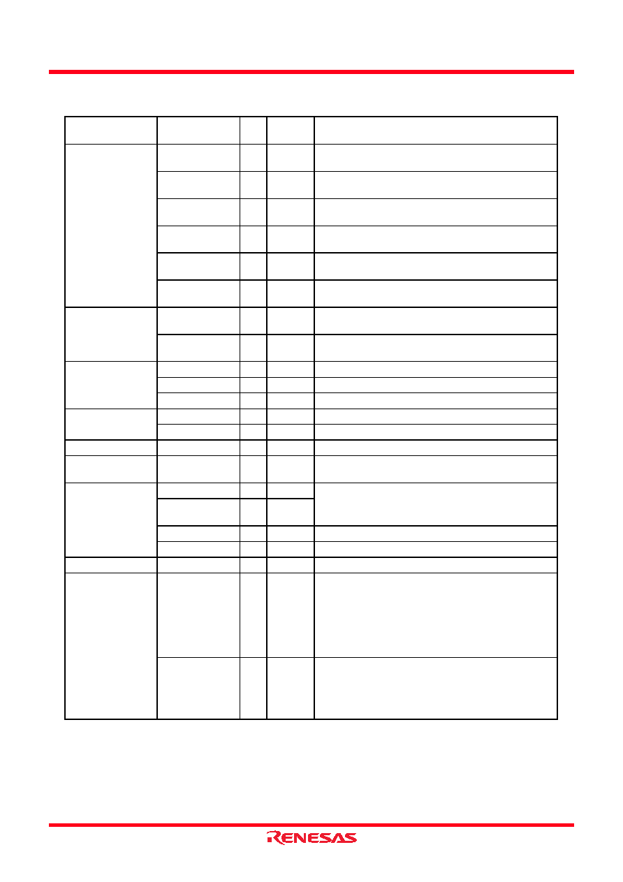
Table 1.14
Pin Functions for the 80-Pin Package (2/2)
Signal Name
Pin Name
I/O
Power
Supply
Description
Serial interface
UART0 to UART2,
UART5
CTS0, CTS1,
CTS5
I
VCC1
Input pins to control data transmission
RTS0, RTS1,
RTS5
O
VCC1
Output pins to control data reception
CLK0, CLK1,
CLK5
I/O
VCC1
Transmit/receive clock I/O.
RXD0 to RXD2,
RXD5
I
VCC1
Serial data input.
TXD0 to TXD2,
TXD5
O
VCC1
Serial data output. (1)
CLKS1
O
VCC1
Output for the transmit/receive clock multiple-pin output
function.
UART0 to UART2,
UART5
I2C mode
SDA0 to SDA2,
SDA5
I/O
VCC1
Serial data I/O for I2C mode.
SCL0 to SCL2,
SCL5
I/O
VCC1
Transmit/receive clock I/O for I2C mode.
Serial interface
SI/O3, SI/O4
CLK3, CLK4
I/O
VCC1
Transmit/receive clock I/O.
SIN4
I
VCC1
Serial data input.
SOUT3, SOUT4
O
VCC1
Serial data output.
Multi-master I2C-bus
interface
SDAMM
I/O
VCC1
Serial data I/O (N-channel open drain output).
SCLMM
I/O
VCC1
Transmit/receive clock I/O (N-channel open drain output).
CEC I/O
CEC
I/O
VCC1
CEC I/O (N-channel open drain output).
Reference voltage
input
VREF
I
VCC1
Reference voltage input for the A/D and D/A converters.
A/D converter
AN0 to AN7
I
VCC1
Analog input for the A/D converter.
AN0_0 to AN0_7
AN2_0 to AN2_7
I
VCC1
ADTRG
I
VCC1
Input for an external A/D trigger.
ANEX0, ANEX1
I
VCC1
Extended analog input for the A/D converter.
D/A converter
DA0, DA1
O
VCC1
Output for the D/A converter.
I/O ports
P0_0 to P0_7
P2_0 to P2_7
P3_0 to P3_7
P5_0 to P5_7
P6_0 to P6_7
P8_0 to P8_7
P10_0 to P10_7
I/O
VCC1
8-bit CMOS I/O ports. A direction register determines
whether each pin is used as an input port or an output
port. A pull-up resistor may be enabled or disabled for
input ports in 4-bit units. P8_5 is an N-channel open drain
output port. No pull-up resistor is provided. P8_5 is an
input port for verifying the
NMI pin level and shares a pin
with
NMI.
P4_0 to P4_3
P7_0, P7_1
P7_6, P7_7
P9_0,
P9_2 to P9_7
I/O
VCC1
I/O ports having equivalent functions to P0. However,
P7_0 and P7_1 are N-channel open drain output ports.
No pull-up resistor is provided.
相關(guān)PDF資料 |
PDF描述 |
|---|---|
| R5F363A6NFB | 16-BIT, FLASH, 20 MHz, MICROCONTROLLER, PQFP100 |
| RTC-6583 | REAL TIME CLOCK, PDSO24 |
| R5F61644N50FPV | 32-BIT, FLASH, 50 MHz, MICROCONTROLLER, PQFP144 |
| R5F3650EDFA | MICROCONTROLLER, PQFP100 |
| R5F3650EDFB | MICROCONTROLLER, PQFP100 |
相關(guān)代理商/技術(shù)參數(shù) |
參數(shù)描述 |
|---|---|
| R5F363A6NFA_11 | 制造商:RENESAS 制造商全稱:Renesas Technology Corp 功能描述:This MCU consumes low power, and supports operating modes |
| R5F363A6NFB | 制造商:Renesas Electronics Corporation 功能描述: |
| R5F363A6NFB#U0 | 制造商:Renesas Electronics Corporation 功能描述: |
| R5F363A6NLG | 制造商:RENESAS 制造商全稱:Renesas Technology Corp 功能描述:This MCU consumes low power, and supports operating modes |
| R5F363AEDFA | 制造商:RENESAS 制造商全稱:Renesas Technology Corp 功能描述:RENESAS MCU |
發(fā)布緊急采購,3分鐘左右您將得到回復(fù)。