- 您現(xiàn)在的位置:買賣IC網(wǎng) > PDF目錄230911 > R5F363A6NFA 16-BIT, FLASH, 20 MHz, MICROCONTROLLER, PQFP100 PDF資料下載
參數(shù)資料
| 型號(hào): | R5F363A6NFA |
| 元件分類: | 微控制器/微處理器 |
| 英文描述: | 16-BIT, FLASH, 20 MHz, MICROCONTROLLER, PQFP100 |
| 封裝: | 14 X 20 MM, 0.65 MM PITCH, PLASTIC, QFP-100 |
| 文件頁(yè)數(shù): | 39/115頁(yè) |
| 文件大?。?/td> | 2363K |
| 代理商: | R5F363A6NFA |
第1頁(yè)第2頁(yè)第3頁(yè)第4頁(yè)第5頁(yè)第6頁(yè)第7頁(yè)第8頁(yè)第9頁(yè)第10頁(yè)第11頁(yè)第12頁(yè)第13頁(yè)第14頁(yè)第15頁(yè)第16頁(yè)第17頁(yè)第18頁(yè)第19頁(yè)第20頁(yè)第21頁(yè)第22頁(yè)第23頁(yè)第24頁(yè)第25頁(yè)第26頁(yè)第27頁(yè)第28頁(yè)第29頁(yè)第30頁(yè)第31頁(yè)第32頁(yè)第33頁(yè)第34頁(yè)第35頁(yè)第36頁(yè)第37頁(yè)第38頁(yè)當(dāng)前第39頁(yè)第40頁(yè)第41頁(yè)第42頁(yè)第43頁(yè)第44頁(yè)第45頁(yè)第46頁(yè)第47頁(yè)第48頁(yè)第49頁(yè)第50頁(yè)第51頁(yè)第52頁(yè)第53頁(yè)第54頁(yè)第55頁(yè)第56頁(yè)第57頁(yè)第58頁(yè)第59頁(yè)第60頁(yè)第61頁(yè)第62頁(yè)第63頁(yè)第64頁(yè)第65頁(yè)第66頁(yè)第67頁(yè)第68頁(yè)第69頁(yè)第70頁(yè)第71頁(yè)第72頁(yè)第73頁(yè)第74頁(yè)第75頁(yè)第76頁(yè)第77頁(yè)第78頁(yè)第79頁(yè)第80頁(yè)第81頁(yè)第82頁(yè)第83頁(yè)第84頁(yè)第85頁(yè)第86頁(yè)第87頁(yè)第88頁(yè)第89頁(yè)第90頁(yè)第91頁(yè)第92頁(yè)第93頁(yè)第94頁(yè)第95頁(yè)第96頁(yè)第97頁(yè)第98頁(yè)第99頁(yè)第100頁(yè)第101頁(yè)第102頁(yè)第103頁(yè)第104頁(yè)第105頁(yè)第106頁(yè)第107頁(yè)第108頁(yè)第109頁(yè)第110頁(yè)第111頁(yè)第112頁(yè)第113頁(yè)第114頁(yè)第115頁(yè)
REJ03B0271-0100 Rev.1.00 Sep 15, 2009
Page 3 of 113
M16C/63 Group
1. Overview
Notes:
1.
IEBus is a registered trademark of NEC Electronics Corporation.
2.
See Table 1.5 “Product List” for the operating temperature.
3.
The CEC function indicates circuitry which supports the transmission and reception of CEC signals standardized
by the High-Definition Multimedia Interface (HDMI). HDMI and High-Definition Multimedia Interface are
registered trademarks of HDMI Licensing, LLC.
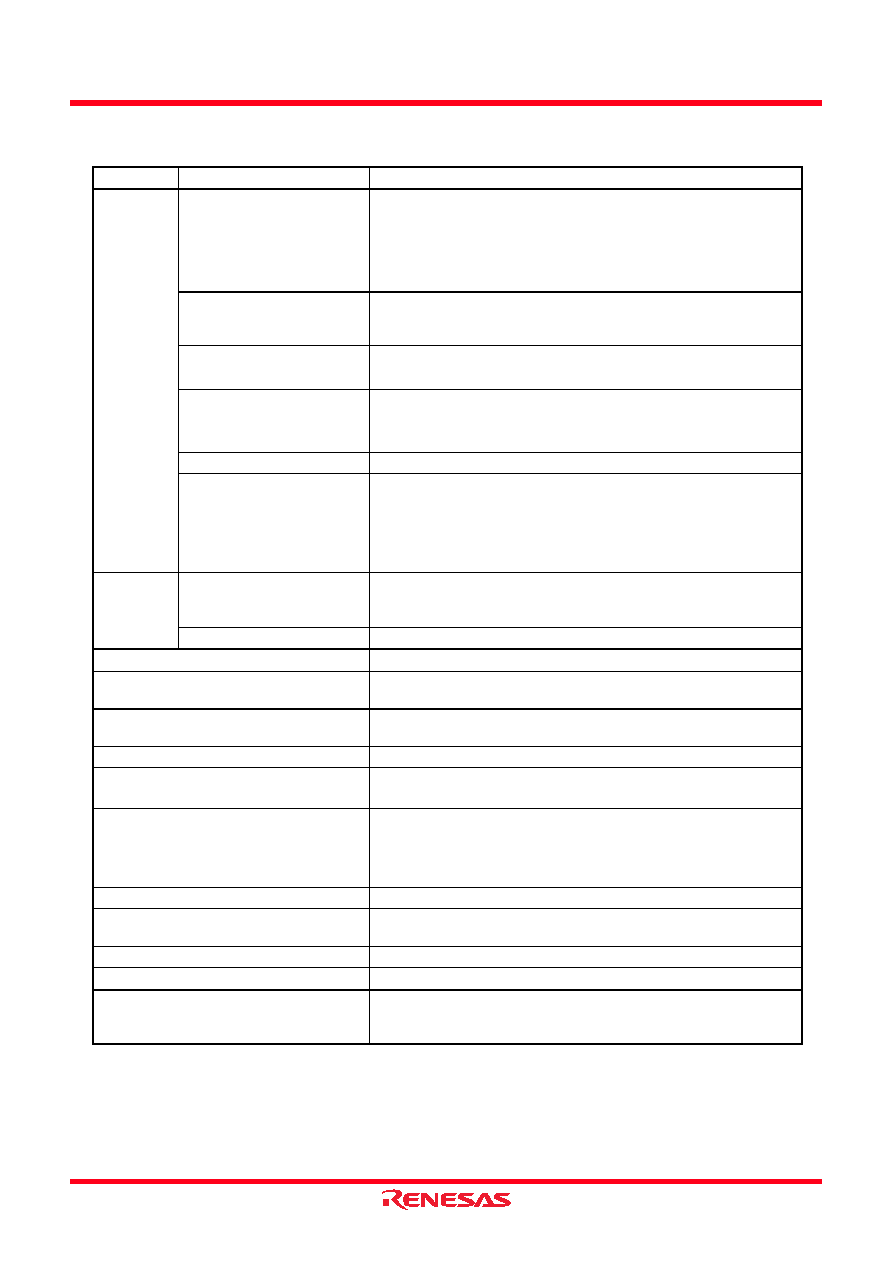
Table 1.2
Specifications for the 100-Pin Package (2/2)
Item
Function
Description
Timers
Timer A
16-bit timer × 5
Timer mode, event counter mode, one-shot timer mode, pulse width
modulation (PWM) mode
Event counter two-phase pulse signal processing (two-phase encoder
input) × 3
Programmable output mode × 3
Timer B
16-bit timer × 6
Timer mode, event counter mode, pulse period measurement mode,
pulse width measurement mode
Three-phase motor control
timer functions
Three-phase inverter control (timer A1, timer A2, timer A4, timer B2)
On-chip dead time timer
Real-time clock
Count: second, minute, hour, day of the week, month, year
Periodic interrupt: 0.25 s, 0.5 s
Automatic correction function
PWM function
8 bits × 2
Remote control signal receiver
2 circuits
4 wave pattern matchings (differentiate wave pattern for headers, data
0, data 1, and special data)
6-byte receive buffer (1 circuit only)
Operating frequency of 32 kHz
Serial
Interface
UART0 to UART2, UART5 to
UART7
Clock synchronous/asynchronous × 6 channels
SIM (UART2)
SI/O3, SI/O4
Clock synchronization only × 2 channels
Multi-master I2C-bus Interface
1 channel
CEC Functions (3)
CEC transmit/receive, arbitration lost detection, ACK automatic output,
operation frequency of 32 kHz
A/D Converter
10-bit resolution × 26 channels, including sample and hold function
Conversion time: 2.15 s
D/A Converter
8-bit resolution × 2 circuits
CRC Calculator
CRC-CCITT (X16 + X12 + X5 + 1),
CRC-16 (X16 + X15 + X2 + 1) compliant
Flash Memory
Erase/write power supply voltage: 2.7 to 5.5 V
Erase/write cycles: 1,000 times (program ROM 1, program ROM 2),
10,000 times (data flash)
Program security: ROM code protect, ID code check
Debug Functions
On-chip debug, on-board flash rewrite, address match interrupt × 4
Operation Frequency/Supply Voltage
5 MHz/VCC1 = 1.8 to 5.5 V, VCC2 = 1.8 V to VCC1
20 MHz/VCC1 = 2.7 to 5.5 V, VCC2 = 2.7 V to VCC1
Current Consumption
Described in 5. “Electrical Characteristics”
Operating Temperature
-20°C to 85°C, -40°C to 85°C (2)
Package
100-pin QFP: PRQP0100JD-B (Previous package code: 100P6F-A)
100-pin LQFP: PLQP0100KB-A (Previous package code: 100P6Q-A)
100-pin LGA: PTLG0100KA-A (Previous package code: 100F0M)
相關(guān)PDF資料 |
PDF描述 |
|---|---|
| R5F363A6NFB | 16-BIT, FLASH, 20 MHz, MICROCONTROLLER, PQFP100 |
| RTC-6583 | REAL TIME CLOCK, PDSO24 |
| R5F61644N50FPV | 32-BIT, FLASH, 50 MHz, MICROCONTROLLER, PQFP144 |
| R5F3650EDFA | MICROCONTROLLER, PQFP100 |
| R5F3650EDFB | MICROCONTROLLER, PQFP100 |
相關(guān)代理商/技術(shù)參數(shù) |
參數(shù)描述 |
|---|---|
| R5F363A6NFA_11 | 制造商:RENESAS 制造商全稱:Renesas Technology Corp 功能描述:This MCU consumes low power, and supports operating modes |
| R5F363A6NFB | 制造商:Renesas Electronics Corporation 功能描述: |
| R5F363A6NFB#U0 | 制造商:Renesas Electronics Corporation 功能描述: |
| R5F363A6NLG | 制造商:RENESAS 制造商全稱:Renesas Technology Corp 功能描述:This MCU consumes low power, and supports operating modes |
| R5F363AEDFA | 制造商:RENESAS 制造商全稱:Renesas Technology Corp 功能描述:RENESAS MCU |
發(fā)布緊急采購(gòu),3分鐘左右您將得到回復(fù)。