- 您現(xiàn)在的位置:買賣IC網(wǎng) > PDF目錄378056 > PM73488-PI (PMC-SIERRA INC) 5 Gbit/s ATM Switch Fabric Element PDF資料下載
參數(shù)資料
| 型號: | PM73488-PI |
| 廠商: | PMC-SIERRA INC |
| 元件分類: | 數(shù)字傳輸電路 |
| 英文描述: | 5 Gbit/s ATM Switch Fabric Element |
| 中文描述: | ATM SWITCHING CIRCUIT, PBGA596 |
| 封裝: | EPBGA-596 |
| 文件頁數(shù): | 84/135頁 |
| 文件大小: | 1735K |
| 代理商: | PM73488-PI |
第1頁第2頁第3頁第4頁第5頁第6頁第7頁第8頁第9頁第10頁第11頁第12頁第13頁第14頁第15頁第16頁第17頁第18頁第19頁第20頁第21頁第22頁第23頁第24頁第25頁第26頁第27頁第28頁第29頁第30頁第31頁第32頁第33頁第34頁第35頁第36頁第37頁第38頁第39頁第40頁第41頁第42頁第43頁第44頁第45頁第46頁第47頁第48頁第49頁第50頁第51頁第52頁第53頁第54頁第55頁第56頁第57頁第58頁第59頁第60頁第61頁第62頁第63頁第64頁第65頁第66頁第67頁第68頁第69頁第70頁第71頁第72頁第73頁第74頁第75頁第76頁第77頁第78頁第79頁第80頁第81頁第82頁第83頁當前第84頁第85頁第86頁第87頁第88頁第89頁第90頁第91頁第92頁第93頁第94頁第95頁第96頁第97頁第98頁第99頁第100頁第101頁第102頁第103頁第104頁第105頁第106頁第107頁第108頁第109頁第110頁第111頁第112頁第113頁第114頁第115頁第116頁第117頁第118頁第119頁第120頁第121頁第122頁第123頁第124頁第125頁第126頁第127頁第128頁第129頁第130頁第131頁第132頁第133頁第134頁第135頁
PMC-Sierra, Inc.
PM73488 QSE
L
PMC-980616
Issue 3
5 Gbit/s ATMSwitch Fabric Element
Released
Datasheet
86
8
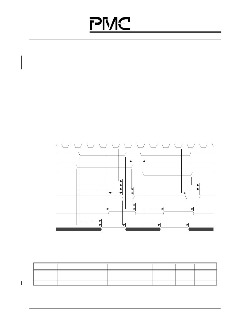
TIMING DIAGRAMS
All signal names are described in
section 6.4 “Pin Descriptions” starting on page 70
. Unless otherwise indicated, all
output timing delays assume a capacitive loading of 30 pF and that the internal PLL is enabled. The use of the internal
PLL is controlled through the /PLL_BYPASS signal. It is recommended that the internal PLL remains enabled
8.1
A microprocessor cycle starts when the chip select (/CS) and either read (/RD) or write (/WR) are asserted. During
read cycles, the QSE asserts /ACK to indicate data on the data bus is valid, and during write cycles the QSE asserts /
ACK to indicate the write has finished and data can be removed from the bus. The microprocessor can terminate the
current cycle at anytime. As shown in Figure 37, the QSE stops driving the data bus and deasserts the /ACK control
line when the cycle terminates. The current cycle terminates when the chip select is deasserted, or when both read and
write are deasserted. A new cycle can start once the /ACK has been deasserted. If the cycle was terminated prema-
turely before the /ACK was asserted, then a new microprocessor cycle can start after one clock cycle.
Microprocessor Timing
NOTE: Asserting both read and write lines together while the chip select is asserted (/RD = 0, /WR = 0, and /
CS = 0) will cause the device to operate in an undefined manner.
Figure 37. Microprocessor Timing
Table 27.
Microprocessor Timing
Symbol
Parameter
Conditions
Min
Max
Unit
/ACK valid after /CS, /RD, or /
WR, whichever is low last
SE_CLK-to-output delay
/ACK
2
118
SE_CLK
cycles
ns
Tqk
/ACK
1
10
Twcy
Tvdk
Tqk
Tvk
Tvk
Thc
Thc
Tqk
Thc
Thc
Tqd
Thc
Thc
Tvd
Thd
Tva
Tva
Tha
Tva
Tha
SE_CLK
/CS
/RD
/WR
/ACK
DATA(7:0)
ADD(7:0)
相關PDF資料 |
PDF描述 |
|---|---|
| PM73488 | 5 Gbit/s ATM Switch Fabric Element |
| PM7349 | Ultraframer DS3/E3/DS2/E2/DS1/E1/DS0 |
| PM7350 | Dual Serial Link, PHY Multiplexer |
| PM7350-PI | DUAL SERIAL LINK PHY MULTIPLEXER |
| PM7351 | OCTAL SERIAL LINK MULTIPLEXER |
相關代理商/技術參數(shù) |
參數(shù)描述 |
|---|---|
| PM7349 | 制造商:PMC 制造商全稱:PMC 功能描述:Quad J2, E3 and DS-3 Framer |
| PM7349-BI | 制造商:未知廠家 制造商全稱:未知廠家 功能描述:Telecommunication IC |
| PM7350 | 制造商:PMC 制造商全稱:PMC 功能描述:DUAL SERIAL LINK PHY MULTIPLEXER |
發(fā)布緊急采購,3分鐘左右您將得到回復。