- 您現(xiàn)在的位置:買(mǎi)賣(mài)IC網(wǎng) > PDF目錄378055 > PM7347 (PMC-Sierra, Inc.) SATURN USER NETWORK INTERFACE for J2/E3/T3 PDF資料下載
參數(shù)資料
| 型號(hào): | PM7347 |
| 廠商: | PMC-Sierra, Inc. |
| 英文描述: | SATURN USER NETWORK INTERFACE for J2/E3/T3 |
| 中文描述: | 土星用戶網(wǎng)絡(luò)接口的J2/E3/T3 |
| 文件頁(yè)數(shù): | 260/341頁(yè) |
| 文件大?。?/td> | 1861K |
| 代理商: | PM7347 |
第1頁(yè)第2頁(yè)第3頁(yè)第4頁(yè)第5頁(yè)第6頁(yè)第7頁(yè)第8頁(yè)第9頁(yè)第10頁(yè)第11頁(yè)第12頁(yè)第13頁(yè)第14頁(yè)第15頁(yè)第16頁(yè)第17頁(yè)第18頁(yè)第19頁(yè)第20頁(yè)第21頁(yè)第22頁(yè)第23頁(yè)第24頁(yè)第25頁(yè)第26頁(yè)第27頁(yè)第28頁(yè)第29頁(yè)第30頁(yè)第31頁(yè)第32頁(yè)第33頁(yè)第34頁(yè)第35頁(yè)第36頁(yè)第37頁(yè)第38頁(yè)第39頁(yè)第40頁(yè)第41頁(yè)第42頁(yè)第43頁(yè)第44頁(yè)第45頁(yè)第46頁(yè)第47頁(yè)第48頁(yè)第49頁(yè)第50頁(yè)第51頁(yè)第52頁(yè)第53頁(yè)第54頁(yè)第55頁(yè)第56頁(yè)第57頁(yè)第58頁(yè)第59頁(yè)第60頁(yè)第61頁(yè)第62頁(yè)第63頁(yè)第64頁(yè)第65頁(yè)第66頁(yè)第67頁(yè)第68頁(yè)第69頁(yè)第70頁(yè)第71頁(yè)第72頁(yè)第73頁(yè)第74頁(yè)第75頁(yè)第76頁(yè)第77頁(yè)第78頁(yè)第79頁(yè)第80頁(yè)第81頁(yè)第82頁(yè)第83頁(yè)第84頁(yè)第85頁(yè)第86頁(yè)第87頁(yè)第88頁(yè)第89頁(yè)第90頁(yè)第91頁(yè)第92頁(yè)第93頁(yè)第94頁(yè)第95頁(yè)第96頁(yè)第97頁(yè)第98頁(yè)第99頁(yè)第100頁(yè)第101頁(yè)第102頁(yè)第103頁(yè)第104頁(yè)第105頁(yè)第106頁(yè)第107頁(yè)第108頁(yè)第109頁(yè)第110頁(yè)第111頁(yè)第112頁(yè)第113頁(yè)第114頁(yè)第115頁(yè)第116頁(yè)第117頁(yè)第118頁(yè)第119頁(yè)第120頁(yè)第121頁(yè)第122頁(yè)第123頁(yè)第124頁(yè)第125頁(yè)第126頁(yè)第127頁(yè)第128頁(yè)第129頁(yè)第130頁(yè)第131頁(yè)第132頁(yè)第133頁(yè)第134頁(yè)第135頁(yè)第136頁(yè)第137頁(yè)第138頁(yè)第139頁(yè)第140頁(yè)第141頁(yè)第142頁(yè)第143頁(yè)第144頁(yè)第145頁(yè)第146頁(yè)第147頁(yè)第148頁(yè)第149頁(yè)第150頁(yè)第151頁(yè)第152頁(yè)第153頁(yè)第154頁(yè)第155頁(yè)第156頁(yè)第157頁(yè)第158頁(yè)第159頁(yè)第160頁(yè)第161頁(yè)第162頁(yè)第163頁(yè)第164頁(yè)第165頁(yè)第166頁(yè)第167頁(yè)第168頁(yè)第169頁(yè)第170頁(yè)第171頁(yè)第172頁(yè)第173頁(yè)第174頁(yè)第175頁(yè)第176頁(yè)第177頁(yè)第178頁(yè)第179頁(yè)第180頁(yè)第181頁(yè)第182頁(yè)第183頁(yè)第184頁(yè)第185頁(yè)第186頁(yè)第187頁(yè)第188頁(yè)第189頁(yè)第190頁(yè)第191頁(yè)第192頁(yè)第193頁(yè)第194頁(yè)第195頁(yè)第196頁(yè)第197頁(yè)第198頁(yè)第199頁(yè)第200頁(yè)第201頁(yè)第202頁(yè)第203頁(yè)第204頁(yè)第205頁(yè)第206頁(yè)第207頁(yè)第208頁(yè)第209頁(yè)第210頁(yè)第211頁(yè)第212頁(yè)第213頁(yè)第214頁(yè)第215頁(yè)第216頁(yè)第217頁(yè)第218頁(yè)第219頁(yè)第220頁(yè)第221頁(yè)第222頁(yè)第223頁(yè)第224頁(yè)第225頁(yè)第226頁(yè)第227頁(yè)第228頁(yè)第229頁(yè)第230頁(yè)第231頁(yè)第232頁(yè)第233頁(yè)第234頁(yè)第235頁(yè)第236頁(yè)第237頁(yè)第238頁(yè)第239頁(yè)第240頁(yè)第241頁(yè)第242頁(yè)第243頁(yè)第244頁(yè)第245頁(yè)第246頁(yè)第247頁(yè)第248頁(yè)第249頁(yè)第250頁(yè)第251頁(yè)第252頁(yè)第253頁(yè)第254頁(yè)第255頁(yè)第256頁(yè)第257頁(yè)第258頁(yè)第259頁(yè)當(dāng)前第260頁(yè)第261頁(yè)第262頁(yè)第263頁(yè)第264頁(yè)第265頁(yè)第266頁(yè)第267頁(yè)第268頁(yè)第269頁(yè)第270頁(yè)第271頁(yè)第272頁(yè)第273頁(yè)第274頁(yè)第275頁(yè)第276頁(yè)第277頁(yè)第278頁(yè)第279頁(yè)第280頁(yè)第281頁(yè)第282頁(yè)第283頁(yè)第284頁(yè)第285頁(yè)第286頁(yè)第287頁(yè)第288頁(yè)第289頁(yè)第290頁(yè)第291頁(yè)第292頁(yè)第293頁(yè)第294頁(yè)第295頁(yè)第296頁(yè)第297頁(yè)第298頁(yè)第299頁(yè)第300頁(yè)第301頁(yè)第302頁(yè)第303頁(yè)第304頁(yè)第305頁(yè)第306頁(yè)第307頁(yè)第308頁(yè)第309頁(yè)第310頁(yè)第311頁(yè)第312頁(yè)第313頁(yè)第314頁(yè)第315頁(yè)第316頁(yè)第317頁(yè)第318頁(yè)第319頁(yè)第320頁(yè)第321頁(yè)第322頁(yè)第323頁(yè)第324頁(yè)第325頁(yè)第326頁(yè)第327頁(yè)第328頁(yè)第329頁(yè)第330頁(yè)第331頁(yè)第332頁(yè)第333頁(yè)第334頁(yè)第335頁(yè)第336頁(yè)第337頁(yè)第338頁(yè)第339頁(yè)第340頁(yè)第341頁(yè)
S/UNI-JET Data Sheet
Released
Proprietary and Confidential to PMC-Sierra, Inc., and for its Customers’ Internal Use
Document ID: PMC-1990267, Issue 3
260
Set the S/UNI-JET Transmit Cell Processor block built in set test (BIST) controls signals by
writing:
°
10000000 to test register 480H
°
10000000 to test register 580H
°
10000000 to test register 680H
°
10000000 to test register 780H
°
10101010 to test register 482H
°
10101010 to test register 582H
°
10101010 to test register 682H
°
10101010 to test register 782H
Toggle REF8KI (pin T3, datasheet page 29) signal several times. This provides the clock to
the RAM. REF8KI is the test clock used by the TXCP and RXCP blocks when in test mode.
Set IOTST (bit 2) in the Master Test Register (datasheet pg. 291) to '0' (by writing 00000000
to Register 400H).
Resume normal device programming.
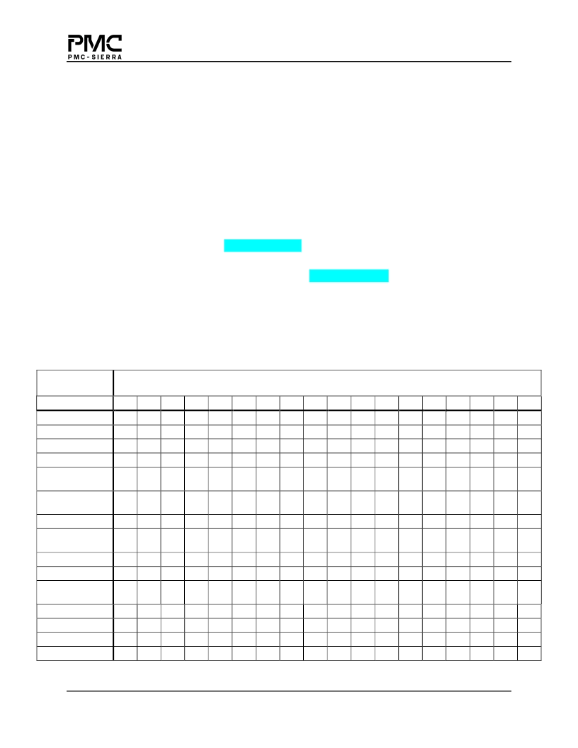
13.2
Register Settings for Basic Configurations
Table 33 Register Settings for Basic Configurations
Mode of
Operation
S/UNI-JET Registers (values in Hexadecimal)
300
302
303
304
308
30C
330
334
338
339
340
341
344
34C
360
361
380
39B
T3 C-bit ADM
C0
00
00
F8
00
00
83
01
--
--
--
--
--
--
04
04
04
00
T3 M23 ADM
C0
00
00
F8
00
00
82
00
--
--
--
--
--
--
04
04
04
00
T3 C-bit PLCP
40
00
00
F8
04
04
83
01
--
--
--
--
--
--
04
00
04
00
T3 M23 PLCP
40
00
00
F8
04
04
82
00
--
--
--
--
--
--
04
00
04
00
T3 C-bit framer
only
50
00
00
78
00
00
83
01
--
--
--
--
--
--
--
--
--
01
T3 M23 framer
only
50
00
00
78
00
00
82
00
--
--
--
--
--
--
--
--
--
01
E3 G.832 ADM
C0
40
40
F8
00
00
--
--
04
00
01
01
--
--
04
08
04
00
E3 G.832 framer
only
50
40
40
78
00
00
--
--
04
00
01
01
--
--
--
--
--
01
E3 G.751 ADM
C0
40
40
F8
00
44
--
--
00
00
00
41
--
--
04
08
04
00
E3 G.751 PLCP
40
40
40
F8
44
44
--
--
00
04
00
41
--
--
04
00
04
00
E3 G.751 framer
only
50
40
40
78
00
00
--
--
00
00
00
01
--
--
--
--
--
01
J2 ADM
J2 framer only
1
C0
80
80
F8
00
00
--
--
--
--
--
03
0E
04
08
04
00
50
80
80
78
00
00
--
--
--
--
--
03
0E
--
--
01
E1 PLCP
40
C0
C0
--
C4
C4
--
--
--
--
--
--
--
04
00
04
00
E1 ADM
40
C0
C0
--
C0
C0
--
--
--
--
--
--
--
04
00
04
00
相關(guān)PDF資料 |
PDF描述 |
|---|---|
| PM7347-BI | SATURN USER NETWORK INTERFACE for J2/E3/T3 |
| PM73487-PI | 622 Mbps ATM Traffic Management Device |
| PM73487 | 622 Mbps ATM Traffic Management Device |
| PM73488-PI | 5 Gbit/s ATM Switch Fabric Element |
| PM73488 | 5 Gbit/s ATM Switch Fabric Element |
相關(guān)代理商/技術(shù)參數(shù) |
參數(shù)描述 |
|---|---|
| PM7347-BI | 制造商:PMC 制造商全稱:PMC 功能描述:SATURN USER NETWORK INTERFACE for J2/E3/T3 |
| PM7347S | 制造商:未知廠家 制造商全稱:未知廠家 功能描述:Telecommunication IC |
| PM73487 | 制造商:PMC 制造商全稱:PMC 功能描述:622 Mbps ATM Traffic Management Device |
發(fā)布緊急采購(gòu),3分鐘左右您將得到回復(fù)。