- 您現在的位置:買賣IC網 > PDF目錄69040 > MSM9225BGA-2K (OKI ELECTRIC INDUSTRY CO LTD) 2 CHANNEL(S), 1M bps, LOCAL AREA NETWORK CONTROLLER, PQFP44 PDF資料下載
參數資料
| 型號: | MSM9225BGA-2K |
| 廠商: | OKI ELECTRIC INDUSTRY CO LTD |
| 元件分類: | 微控制器/微處理器 |
| 英文描述: | 2 CHANNEL(S), 1M bps, LOCAL AREA NETWORK CONTROLLER, PQFP44 |
| 封裝: | PLASTIC, QFP-44 |
| 文件頁數: | 62/95頁 |
| 文件大?。?/td> | 567K |
| 代理商: | MSM9225BGA-2K |
第1頁第2頁第3頁第4頁第5頁第6頁第7頁第8頁第9頁第10頁第11頁第12頁第13頁第14頁第15頁第16頁第17頁第18頁第19頁第20頁第21頁第22頁第23頁第24頁第25頁第26頁第27頁第28頁第29頁第30頁第31頁第32頁第33頁第34頁第35頁第36頁第37頁第38頁第39頁第40頁第41頁第42頁第43頁第44頁第45頁第46頁第47頁第48頁第49頁第50頁第51頁第52頁第53頁第54頁第55頁第56頁第57頁第58頁第59頁第60頁第61頁當前第62頁第63頁第64頁第65頁第66頁第67頁第68頁第69頁第70頁第71頁第72頁第73頁第74頁第75頁第76頁第77頁第78頁第79頁第80頁第81頁第82頁第83頁第84頁第85頁第86頁第87頁第88頁第89頁第90頁第91頁第92頁第93頁第94頁第95頁
MSM9225B User’s Manual
Chapter 4 Microcontroller Interface
4 – 1
Chapter 4
Microcontroller Interface
There are two methods of interfacing to the microcontroller.
(1) Synchronous serial interface (serial mode)
(2) Parallel bus interface (parallel mode)
Each interface is selected with the Mode1 and Mode0 pins.
Table 4-1 shows the relation between Mode1 and Mode0 pin values and interface selection.
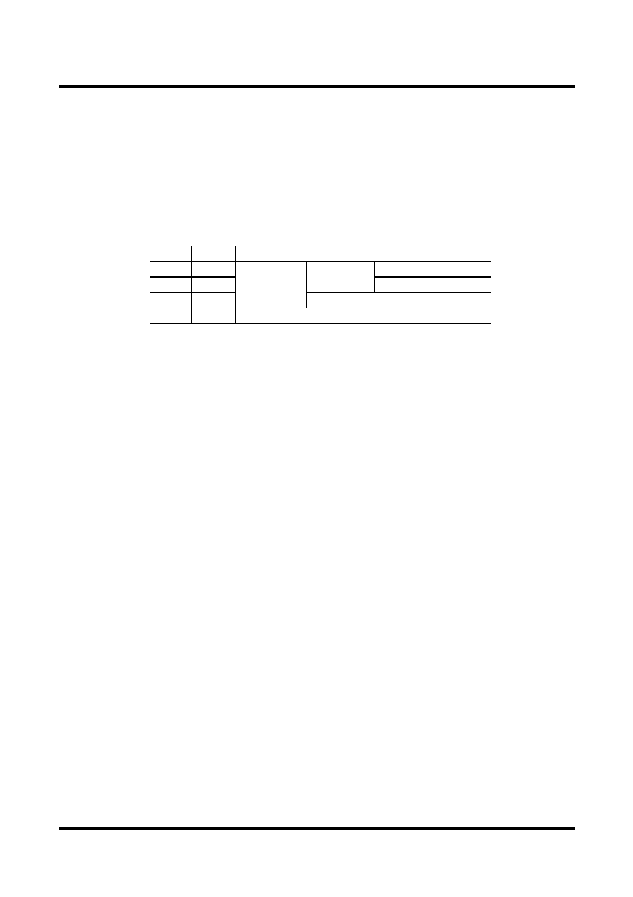
Table 4-1 Interface Setting
Mode1
Mode0
Interface
0
No address latch signal
01
Separate
buses
With address latch signal
10
Parallel mode
Multiplexed buses
11
Serial mode
4.1
Serial Interface
Figure 4-1 shows the transfer timing.
Address/data transfers begin when the
CS pin is at a “L” level and end when it changes to a “H” level. Because the
MSM9225B has an address increment function, the basic transfer consists of “ transfer start address + multiple
data.” Therefore, to access a nonconsecutive address, the
CS must be first pulled to a “H” level, and then the
address set.
Perform address/data transfers LSB first, in 8-bit units. During a transfer, an interval is necessary between address
and data and between consecutive data transfers. (Refer to Chapter 5, “Electrical Characteristics”, for interval
values.) Note that the SWAIT signal is only generated during the interval between address and data transfers.
(1) Data write
Data write operations are performed with the following procedure.
After setting the
CS pin and PRD/SRW pin to “L” levels, input an address to the SDI pin. Synchronized to
the rising edge of synchronous clock SCLK, the MSM9225B captures the address in an internal register.
When 8 SCLK clocks are received, the MSM9225B loads the address into the internal address counter and
waits for data reception.
Next, input data to the SDI pin. An internal register captures data in a similar manner to the address capture,
at the rising edge of SCLK. When 8 bits of data have been captured, the MSM9225B writes the data to the
message memory or control register specified by the address that was received previously, and then
increments the address counter by 1. If data is to be written to consecutive addresses, continue the data
transfer. After all data has been transferred, set the
CS pin to a “H” level.
(2) Data read
Data read operations are performed with the following procedure.
After setting the
CS pin to a “L” level and the PRD/SRW pin to a “H” level, input an address to the SDI pin in
the same manner as for the data write operation. When 8 SCLK clocks are received, the MSM9225B loads
the address into the internal address counter, reads data from the message memory or control register
specified by the address, latches data into a shift register for data output and increments the address counter.
Then, when SCLK is input, latched data is output from the SDO pin synchronized to the falling edge of SCLK.
At this time, the contents of the data input from the SDI pin does not matter. If there exists remaining data to
be read, input another 8 SCLK clocks. After all the data at consecutive addresses has been read, set the
CS pin
to a “H” level.
If the count value of the lower 4 bits of an address overflows (exceeds xFh), the address increment function
will reset the count value of the lower 4 bits to 0 without changing the upper 4 bits of the address, and will
continue counting.
相關PDF資料 |
PDF描述 |
|---|---|
| MSP430A003IPW | 16-BIT, FLASH, 8 MHz, RISC MICROCONTROLLER, PDSO20 |
| MSP430A004IPWR | 16-BIT, 8 MHz, RISC MICROCONTROLLER, PDSO20 |
| MSP430A005IPWR | 16-BIT, 8 MHz, RISC MICROCONTROLLER, PDSO28 |
| MSP430A004IPW | 16-BIT, 8 MHz, RISC MICROCONTROLLER, PDSO20 |
| MSP430A019IRHBR | 16-BIT, FLASH, 8 MHz, RISC MICROCONTROLLER, PQCC64 |
相關代理商/技術參數 |
參數描述 |
|---|---|
| MSM9225BGAZ020 | 制造商:ROHM Semiconductor 功能描述: |
| MSM9225BGAZ0VL | 制造商:ROHM Semiconductor 功能描述: |
| MSM9405 | 制造商:OKI 制造商全稱:OKI electronic componets 功能描述:IrDA Communication Controller |
| MSM9552 | 制造商:OKI 制造商全稱:OKI electronic componets 功能描述:LSI for FM Multiplex Data Demodulation |
| MSM9552GS-2K | 制造商:ROHM Semiconductor 功能描述: |
發(fā)布緊急采購,3分鐘左右您將得到回復。