- 您現(xiàn)在的位置:買賣IC網(wǎng) > PDF目錄45329 > MK30X256VMD100R (FREESCALE SEMICONDUCTOR INC) 32-BIT, FLASH, 100 MHz, RISC MICROCONTROLLER, PBGA144 PDF資料下載
參數(shù)資料
| 型號: | MK30X256VMD100R |
| 廠商: | FREESCALE SEMICONDUCTOR INC |
| 元件分類: | 微控制器/微處理器 |
| 英文描述: | 32-BIT, FLASH, 100 MHz, RISC MICROCONTROLLER, PBGA144 |
| 封裝: | 13 X 13 MM, MAPBGA-144 |
| 文件頁數(shù): | 33/72頁 |
| 文件大?。?/td> | 1847K |
| 代理商: | MK30X256VMD100R |
第1頁第2頁第3頁第4頁第5頁第6頁第7頁第8頁第9頁第10頁第11頁第12頁第13頁第14頁第15頁第16頁第17頁第18頁第19頁第20頁第21頁第22頁第23頁第24頁第25頁第26頁第27頁第28頁第29頁第30頁第31頁第32頁當(dāng)前第33頁第34頁第35頁第36頁第37頁第38頁第39頁第40頁第41頁第42頁第43頁第44頁第45頁第46頁第47頁第48頁第49頁第50頁第51頁第52頁第53頁第54頁第55頁第56頁第57頁第58頁第59頁第60頁第61頁第62頁第63頁第64頁第65頁第66頁第67頁第68頁第69頁第70頁第71頁第72頁
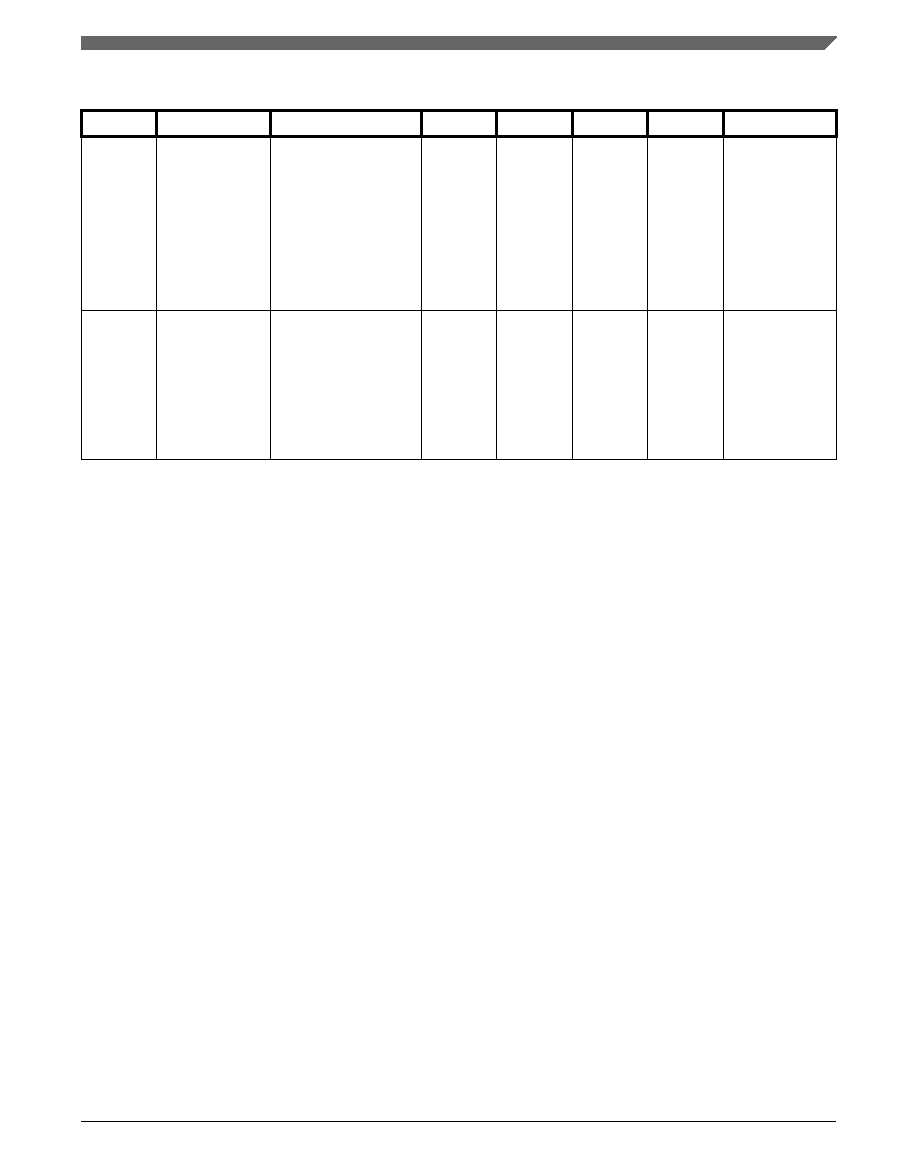
Table 24. 16-bit ADC operating conditions (continued)
Symbol
Description
Conditions
Min.
Max.
Unit
Notes
Crate
ADC conversion
rate
≤13
bit modes
No ADC hardware
averaging
Continuous
conversions enabled
Peripheral clock =
50MHz
18.484
—
818.330
Ksps
Crate
ADC conversion
rate
16 bit modes
No ADC hardware
averaging
Continuous
conversions enabled
Peripheral clock =
50MHz
37.037
—
361.402
Ksps
1. Typical values assume VDDA = 3.0 V, Temp = 25°C, fADCK = 1.0 MHz unless otherwise stated. Typical values are for
reference only and are not tested in production.
2. DC potential difference.
3. This resistance is external to MCU. The analog source resistance should be kept as low as possible in order to achieve the
best results. The results in this datasheet were derived from a system which has <8 Ω analog source resistance. The RAS/
CAS time constant should be kept to <1ns.
4. In order to use the maximum ADC conversion clock frequency ADHSC bit should be set and the ADLPC should be clear.
5. In order to use the maximum ADC conversion clock frequency ADHSC bit should be set and the ADLPC should be clear.
6. For guidelines and examples of conversion rate calculation please download the ADC calculator tool http://
cache.freescale.com/files/soft_dev_tools/software/app_software/converters/ADC_CALCULATOR_CNV.zip?fpsp=1
7. For guidelines and examples of conversion rate calculation please download the ADC calculator tool http://
cache.freescale.com/files/soft_dev_tools/software/app_software/converters/ADC_CALCULATOR_CNV.zip?fpsp=1
Peripheral operating requirements and behaviors
K30 Sub-Family Data Sheet Data Sheet, Rev. 4, 3/2011.
Freescale Semiconductor, Inc.
Preliminary
39
相關(guān)PDF資料 |
PDF描述 |
|---|---|
| MK30N512VLQ100R | 32-BIT, FLASH, 100 MHz, RISC MICROCONTROLLER, PQFP144 |
| MK3200G | 0.032768 MHz, OTHER CLOCK GENERATOR, PDSO8 |
| MK3200S | 0.032768 MHz, OTHER CLOCK GENERATOR, PDSO8 |
| MK3200GLF | 0.032768 MHz, OTHER CLOCK GENERATOR, PDSO8 |
| MK3200SI | 0.032768 MHz, OTHER CLOCK GENERATOR, PDSO8 |
相關(guān)代理商/技術(shù)參數(shù) |
參數(shù)描述 |
|---|---|
| MK310E-DC24 | 制造商:OMRON Electronic Components LLC 功能描述: |
| MK3161F | 制造商:Ohmite Mfg Co 功能描述: |
| MK3-1A66C-500W | 制造商:Meder electronics(Standex) 功能描述: |
| MK3-1C90C-500W | 制造商:Meder electronics(Standex) 功能描述: |
| MK31R6F | 制造商:Ohmite Mfg Co 功能描述: |
發(fā)布緊急采購,3分鐘左右您將得到回復(fù)。