- 您現(xiàn)在的位置:買賣IC網(wǎng) > PDF目錄377931 > MB90V520 (Fujitsu Limited) 16-bit Proprietary Microcontroller PDF資料下載
參數(shù)資料
| 型號: | MB90V520 |
| 廠商: | Fujitsu Limited |
| 英文描述: | 16-bit Proprietary Microcontroller |
| 中文描述: | 16位微控制器專有 |
| 文件頁數(shù): | 29/106頁 |
| 文件大小: | 1539K |
| 代理商: | MB90V520 |
第1頁第2頁第3頁第4頁第5頁第6頁第7頁第8頁第9頁第10頁第11頁第12頁第13頁第14頁第15頁第16頁第17頁第18頁第19頁第20頁第21頁第22頁第23頁第24頁第25頁第26頁第27頁第28頁當(dāng)前第29頁第30頁第31頁第32頁第33頁第34頁第35頁第36頁第37頁第38頁第39頁第40頁第41頁第42頁第43頁第44頁第45頁第46頁第47頁第48頁第49頁第50頁第51頁第52頁第53頁第54頁第55頁第56頁第57頁第58頁第59頁第60頁第61頁第62頁第63頁第64頁第65頁第66頁第67頁第68頁第69頁第70頁第71頁第72頁第73頁第74頁第75頁第76頁第77頁第78頁第79頁第80頁第81頁第82頁第83頁第84頁第85頁第86頁第87頁第88頁第89頁第90頁第91頁第92頁第93頁第94頁第95頁第96頁第97頁第98頁第99頁第100頁第101頁第102頁第103頁第104頁第105頁第106頁
MB90520 Series
29
(Continued)
Descriptions for read/write
R/W: Readable and writable
R: Read only
W: Write only
Descriptions for initial value
0 : The initial value is “0.”
1 : The initial value is “1.”
X : The initial value is indeterminate.
*1: This area is the only external access area having an address of 0000FF
H
or lower. An access operation to this
area is handled as that to external I/O area.
*2: For details of the “RAM area”, see the memory map.
*3: The “reserved area” is basically disabled because it is used in the system.
*4: “Area used by the system” is the area set by the resistor for evaluating tool.
Notes: For bits initialized by reset operations, the initial value set by the reset operation is listed as an initial value.
Note that the values are different from reading results.
For LPMCR/CKSCR/WDTC, there are cases in which initialization is performed or not performed,
depending on the types of the reset. The value listed is the initial value in cases where initialization is per
formed.
The addresses following 0000FF
H
are reserved. No external bus access signal is generated.
Boundary ####
H
between the “RAM area” and the“ reserved area” varies with the product models.
Channels 0 to 3 of the OCU compare register use 16-bit free-run timer 2, while channels 4 to 7 of the OCU
compare register use 16-bit free-run timer 1. 16-bit free-run timer 1 is also used by input captures (ICU)
0 and 1.
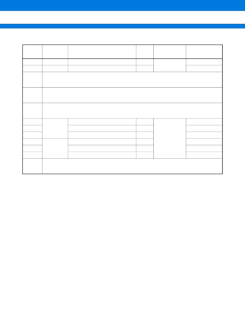
Address
Abbreviated
register
name
ICR14
ICR15
Register name
Read/
write
Resource name
Initial value
0000BE
H
0000BF
H
0000C0
H
to
0000FF
H
000100
H
to
00####
H
00####
H
to
001FEF
H
001FF0
H
001FF1
H
001FF2
H
001FF3
H
001FF4
H
001FF5
H
001FF6
H
to
001FFF
H
Interrupt control register 14
Interrupt control register 15
R/W
R/W
Interrupt
controller
0 0 0 0 0 1 1 1
B
0 0 0 0 0 1 1 1
B
(External area)*
1
(RAM area)*
2
(Reserved area)*
3
PADR0
Program address detection register 0
Program address detection register 1
Program address detection register 2
Program address detection register 3
Program address detection register 4
Program address detection register 5
R/W
R/W
R/W
R/W
R/W
R/W
Address match
detection
function
XXXXXXXX
B
XXXXXXXX
B
XXXXXXXX
B
XXXXXXXX
B
XXXXXXXX
B
XXXXXXXX
B
PADR1
(Reserved area)*
3
相關(guān)PDF資料 |
PDF描述 |
|---|---|
| MB90522 | 36-Bit Bus Transceivers With 3-State Outputs 100-LQFP -55 to 125 |
| MB90522PFF | Quadruple 2-Input Positive-NAND Gates 14-CDIP -55 to 125 |
| MB90522PFV | Quadruple 2-Input Positive-NAND Gates 14-CFP -55 to 125 |
| MB90523 | Quadruple 2-Input Positive-NAND Gates 20-LCCC -55 to 125 |
| MB90523PFF | 16-bit Proprietary Microcontroller |
相關(guān)代理商/技術(shù)參數(shù) |
參數(shù)描述 |
|---|---|
| MB-910 | 制造商:Circuit Test 功能描述:BREADBOARD WIRING KIT - 350 PCS |
| MB9100100 | 制造商:COM/DUO 功能描述:FAN 4-6WKS |
| MB9100-100 | 制造商:COM/DUO 功能描述:FAN 4-6WKS |
| MB91101 | 制造商:Panasonic Industrial Company 功能描述:IC |
| MB91101A | 制造商:FUJITSU 制造商全稱:Fujitsu Component Limited. 功能描述:32-bit RISC Microcontroller |
發(fā)布緊急采購,3分鐘左右您將得到回復(fù)。