- 您現(xiàn)在的位置:買賣IC網(wǎng) > PDF目錄17043 > M52277EVB (Freescale Semiconductor)BOARD DEMO FOR MCF5227 PDF資料下載
參數(shù)資料
| 型號(hào): | M52277EVB |
| 廠商: | Freescale Semiconductor |
| 文件頁(yè)數(shù): | 31/46頁(yè) |
| 文件大?。?/td> | 0K |
| 描述: | BOARD DEMO FOR MCF5227 |
| 標(biāo)準(zhǔn)包裝: | 1 |
| 系列: | ColdFire® |
| 類型: | MCU |
| 適用于相關(guān)產(chǎn)品: | MCF52277 |
| 所含物品: | 板 |
第1頁(yè)第2頁(yè)第3頁(yè)第4頁(yè)第5頁(yè)第6頁(yè)第7頁(yè)第8頁(yè)第9頁(yè)第10頁(yè)第11頁(yè)第12頁(yè)第13頁(yè)第14頁(yè)第15頁(yè)第16頁(yè)第17頁(yè)第18頁(yè)第19頁(yè)第20頁(yè)第21頁(yè)第22頁(yè)第23頁(yè)第24頁(yè)第25頁(yè)第26頁(yè)第27頁(yè)第28頁(yè)第29頁(yè)第30頁(yè)當(dāng)前第31頁(yè)第32頁(yè)第33頁(yè)第34頁(yè)第35頁(yè)第36頁(yè)第37頁(yè)第38頁(yè)第39頁(yè)第40頁(yè)第41頁(yè)第42頁(yè)第43頁(yè)第44頁(yè)第45頁(yè)第46頁(yè)
Electrical Characteristics
MCF5227x ColdFire Microprocessor Data Sheet, Rev. 8
Freescale Semiconductor
37
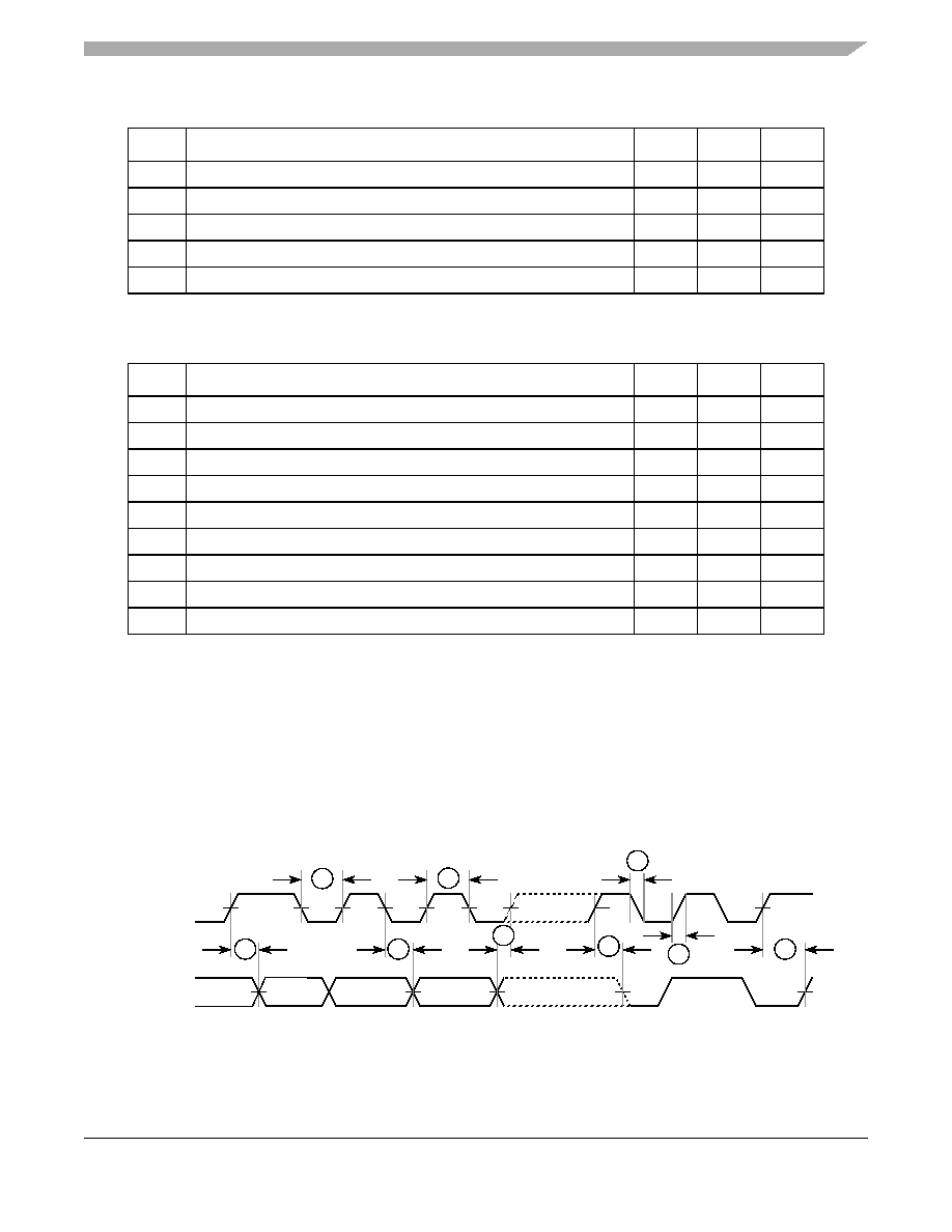
Figure 24. I2C Input/Output Timings
I5
I2C_SCL/I2C_SDA fall time (VIH = 2.4 V to VIL =0.5 V)
—
1
ms
I6
Clock high time
4
—
tcyc
I7
Data setup time
0
—
ns
I8
Start condition setup time (for repeated start condition only)
2
—
tcyc
I9
Stop condition setup time
2
—
tcyc
Table 29. I2C Output Timing Specifications between SCL and SDA
Num
Characteristic
Min
Max
Unit
I11
1 Output numbers depend on the value programmed into the IFDR; an IFDR programmed with the maximum
frequency (IFDR = 0x20) results in minimum output timings as shown in Table 29. The I2C interface is designed
to scale the actual data transition time to move it to the middle of the SCL low period. The actual position is
affected by the prescale and division values programmed into the IFDR; however, the numbers given in Table 29
are minimum values.
Start condition hold time
6
—
tcyc
I21
Clock low period
10
—
tcyc
I32
2 Because I2C_SCL and I2C_SDA are open-collector-type outputs, which the processor can only actively drive
low, the time I2C_SCL or I2C_SDA take to reach a high level depends on external signal capacitance and pull-up
resistor values.
I2C_SCL/I2C_SDA rise time (VIL = 0.5 V to VIH = 2.4 V)
—
s
I41
Data hold time
7
—
tcyc
I53
3 Specified at a nominal 50-pF load.
I2C_SCL/I2C_SDA fall time (VIH = 2.4 V to VIL = 0.5 V)
—
3
ns
I61
Clock high time
10
—
tcyc
I71
Data setup time
2
—
tcyc
I81
Start condition setup time (for repeated start condition only)
20
—
tcyc
I91
Stop condition setup time
10
—
tcyc
Table 28. I2C Input Timing Specifications between SCL and SDA (continued)
Num
Characteristic
Min
Max
Unit
I2
I6
I1
I4
I8
I9
I5
I3
I2C_SCL
I2C_SDA
I7
相關(guān)PDF資料 |
PDF描述 |
|---|---|
| 0210490925 | CABLE JUMPER 1.25MM .076M 23POS |
| ECM12DSEH-S13 | CONN EDGECARD 24POS .156 EXTEND |
| VI-J1R-EY | CONVERTER MINIMOD DC/DC 7.5V 50W |
| VE-21T-EY | CONVERTER MOD DC/DC 6.5V 50W |
| 0210490924 | CABLE JUMPER 1.25MM .076M 23POS |
相關(guān)代理商/技術(shù)參數(shù) |
參數(shù)描述 |
|---|---|
| M5228FP | 制造商:Panasonic Industrial Company 功能描述:IC |
| M5228P | 制造商:Panasonic Industrial Company 功能描述:IC |
| M5229 | 制造商:Panasonic Industrial Company 功能描述:DISCD IC |
| M-522CT | 制造商:NEC 制造商全稱:NEC 功能描述:DC Line Fileters |
| M522D | 制造商:GOSSEN METRAWATT 功能描述:PSI MODULE PROFITEST PSI-BC |
發(fā)布緊急采購(gòu),3分鐘左右您將得到回復(fù)。